Getting Started with KiCad Version 6 : Beginner’s Tutorial to Schematic and PCB Design
Beginner's tutorial to the latest KiCad version 6 open source Electronic Design Automation (EDA) tool. Learn about schematic and PCB designing with KiCad.
There is no better time to learn PCB designing than now. That’s because the most popular open-source EDA (Electronics Design Automation) tool KiCad has just gotten better with the release of version 6. EDA is the process of using software to accelerate electronic designs. This can be schematic design (also called circuit diagram), PCB design, or circuit simulation. Before the era of computers, we used to do this by hand. It was a time-consuming and slow job. Computers make everything magically faster. KiCad is one such advanced software suite for designing electronic circuits and creating PCB layouts from them. It is a suite because it has multiple tools bundled together and is designed to interoperate.
KiCad was originally developed by Jean-Pierre Charras and is now being actively maintained by him and a group of developers. It has everything needed to create complex multi-layer PCBs as you want. It has almost limitless customization options, thanks to the open-source design and scripting tools. KiCad is not the only EDA tool available out there. There are a dozen or more like it. But what makes KiCad special is that it is free to download and open source. Free to download means, you don’t need to pay for a license or subscription. You can keep the software as long as you want and use it for any purpose. Open source means the source code written for the application is publicly available so that you can learn how it works inside, and make modifications as you wish. There are no restrictions to what you can do with it, except a few open-source guidelines specified by GPL (GNU General Public License) to follow. This is the opposite of paid/proprietary software. You have to pay hundreds of dollars to purchase other EDA tools to get the same functionalities as KiCad. Sometimes you have to pay every month or year for a subscription. This means, that once you stop subscribing, you will lose access to new features or the complete software. Not only that, proprietary software has closed source code as opposed to open-source code. This means you won’t be able to see the actual source code of the software or modify it even if you want to. In brief, you are totally at the mercy of the company you’re paying to.
But if you do not have to pay for a free and open-source tool, how do the developers find the money to pay all the expenses? How can they keep spending their time and expertise developing free stuff? That’s where the great generosity of human beings comes into the picture. Most open-source software are developed by their authors in their free time. Others find money through sponsorships and donations. KiCad works like that. They accept donations from individuals around the world and sponsorships from businesses that usually use KiCad for their operations. You can also become a donator. Consider donating to KiCad to keep the development active.
In this tutorial, we will show you how you can create a complete schematic and convert it to a PCB format ready for fabrication. We will use the latest KiCad version 6 on a Windows computer. We have a complete installation tutorial here – How to Install KiCad Version 6 and Organize Part Libraries – which you can use as a guide. Follow the first part if you’re installing fresh.
- Why KiCad?
- What’s Inside KiCad Suite?
- Plugins
- Themes
- Keyboard Shortcuts
- Schematic Editor
- PCB Editor
- Versioning
- Links
- Short Link
Want professionally designed PCBs?
CIRCUITSTATE can turn your bare circuits into complex multi-layer PCBs with the highest performance and quality using industry-leading tools. We can also reverse-engineer your existing products to create accurate schematics and PCB layouts. Contact us today to share your requirements.
Why KiCad?
Before we begin, we must explain why you should learn and use KiCad. We have already explained some aspects of open source philosophy but let us list everything down.
- Free to Download – You don’t have to pay anything for downloading and using KiCad. You can donate to KiCad but that is completely up to you. Nobody will force you to donate or disturb you with constant emails or pop-ups. You can always work worry-free.
- Open Source – Download the complete source code from KiCad’s official repository at Gitlab. Fork the project if you want to add more features and merge them to the official KiCad. You can also join the worldwide community of developers and collaborate with them in development.
- Open Formats and Industry Standards – KiCad uses easy-to-understand text-based file formats for all files. This is unlike proprietary formats that are openable only by their respective software. KiCad files are also supported across industries, thanks to the support for industry formats such as Gerbers.
- Open Part Libraries – Similar to the source code, the component libraries of Kicad are also open-source and publicly available. New schematic symbols, footprints, and 3D models created by contributors around the world are added to this library pool so that everyone can download and use them. You can also create new symbols and footprints and submit them to the pool.
- Fast, Reliable and Extensible – KiCad is a lightweight software written mostly in C/C++ and thus runs really fast on all systems while consuming fewer resources. KiCad can use your graphics card to accelerate displaying of graphic elements. KiCad supports Python scripting with which you can extend the features yourself and use them to automate your workflow.
- Cross Platform – KiCad is available for Windows, Linux distros and Mac OS systems. Features added to KiCad will be available to all operating system versions in no time. KiCad project file you create on a Windows machine will be compatible with that inside a Linux computer and vice versa.
What’s Inside KiCad Suite?
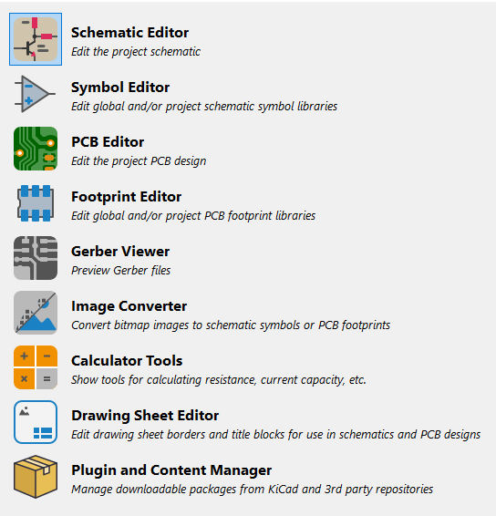
- Schematic Editor – This is the tool you use to draw the circuit diagram or a schematic diagram.
- Symbol Editor – A schematic consists graphical representations of electronic components and their interconnections. A symbol editor helps us to create new schematic symbols that are not already available in the libraries. For example, if you want to create a new symbol for a motor driver IC, you can define the pinouts and their properties when creating the symbol. This symbol can then be saved to an existing library or a new library. You can also create new symbols by modifying existing schematic symbols.
- PCB Editor – This allows us to create a PCB from the schematic we created. Each schematic symbol will have a corresponding footprint on the PCB file. Interconnections are converted to copper tracks that connect each footprint as per the schematic.
- Footprint Editor – We can create new footprints or modify existing footprints with this tool. We can also modify footprint libraries.
- Gerber Viewer – Gerbers are vector graphic files that contain the data for fabricating your PCBs. This data can be generated from KiCad’s PCB editor. Once generated, the Gerber files can be only opened on a Gerber viewer. This will help you to verify the generated files before sending them to fabrication house.
- Image Converter – Sometimes you want to add custom logos or other graphics to your PCBs that are not available from the libraries. Since KiCad only supports vector formats, you can’t directly import raster graphics. The Image Converter helps you to convert image formats such PNG, JPG etc. to KiCad compatible graphics.
- Calculator Tools – This is a set of handy calculators to find various design parameters such as current carrying capacity and track widths.
- Drawing Sheet Editor – If for some reason the existing worksheets are not suitable for your projects, you can create new ones or modify existing ones.
- Plugin and Content Manager – With this, you can install new plugins and themes developed by various third parties. Plugins give you extra features that are not part of the official KiCad software yet.
Plugins
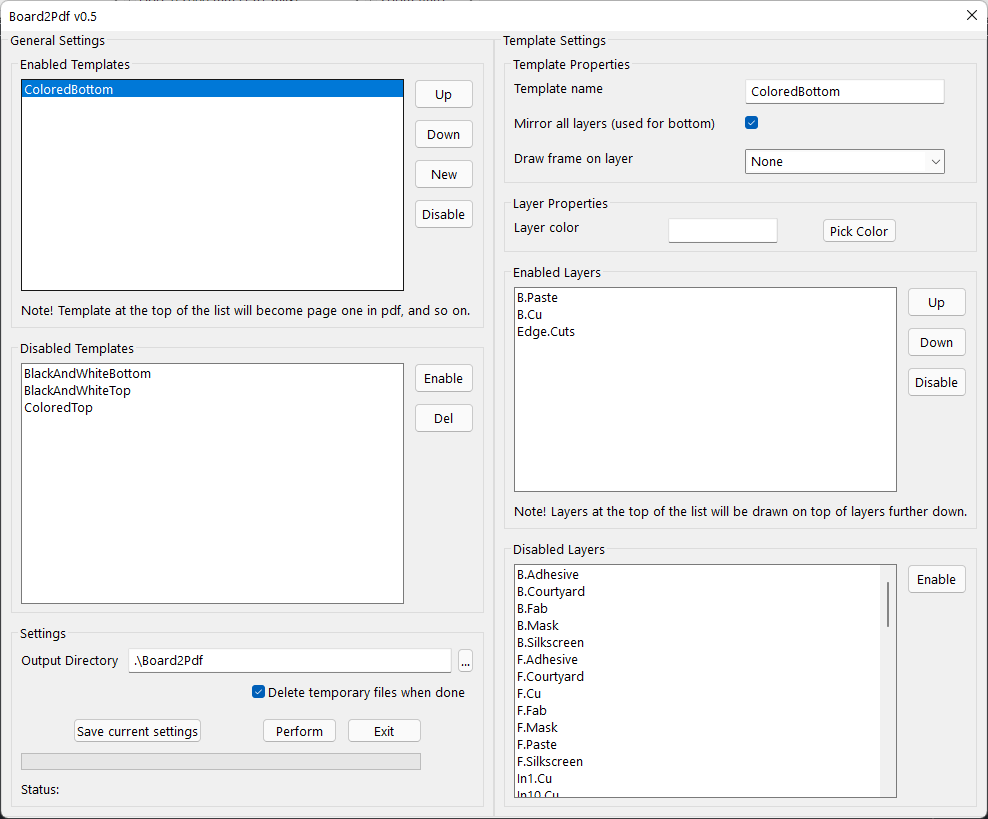
Plugins extend the capabilities of KiCad. Sometimes KiCad’s standard features are not enough or too complicated to get certain things done. For example, this is the case with exporting PDF files. We do not have much control over how the PDF is exported. The Board2Pdf plugin gives us great control of how we can create PDF files from individual PCB layers. We use this plugin to create high-quality PCB graphics easily. Below are some of the must-have plugins supported in KiCad version 6.
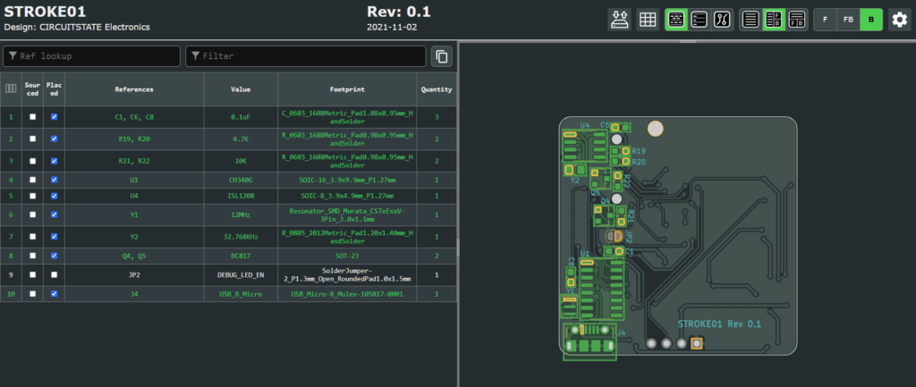
- Interactive HTML BoM – This plugin helps you to create awesome-looking interactive board visualizations and BoM, all in a single HTML file that can be opened in any browser. It can highlight components and nets as you hover or click on them. This tool can be of great help when you’re assembling PCBs manually or want to send the board design to a client who doesn’t have KiCad installed on their system.
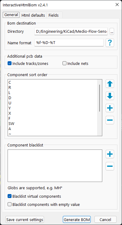
- Board2Pdf – This helps you to export PCB layers as high-quality PDF files in different colors and orders. Extremely useful when you want to create assembly drawings and PCB graphics. This plugin was developed by Albin Dennevi.
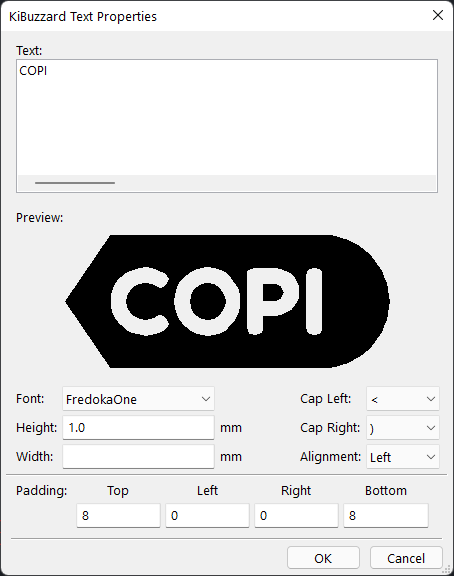
- KiBuzzard – Developed by Greg Davill, this plugin helps you to easily create silkscreen labels in different styles. This is useful when you want to add pin labels and other info that are otherwise difficult to create in KiCad.
- KiKit – This is a great plugin for panelizing PCBs and working with multiple PCB designs on a single project. It was developed by Jan Mrázek.
- PCB-Action-Tools – This is a set of tools to inspect your PCB design and export layers to DXF.
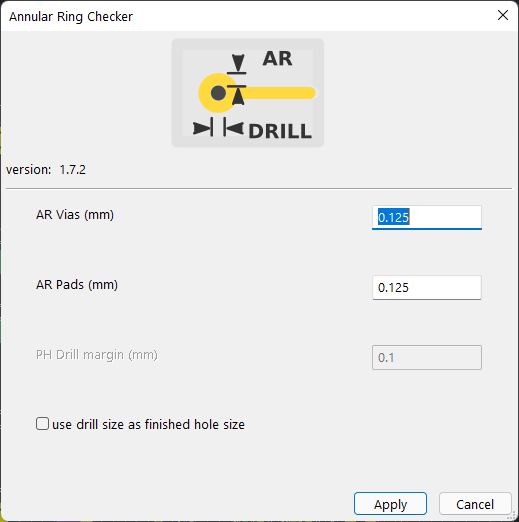
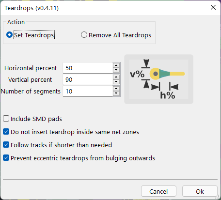
6. Teardrops – This helps you add/remove teardrops to tracks and pads.
7. KiCad Round Tracks – Creates beautiful buttery smooth rounded tracks from your existing tracks.
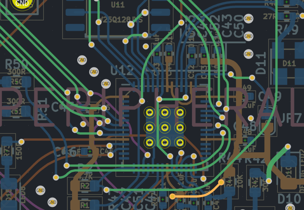
You can install all these plugins through the Plugin and Content Manager (PCM) of KiCad v6. The directory in which the plugins will be installed is determined by the KICAD6_3RD_PARTY variable setting. Make sure you use an accessible path. Users have reported that using a folder that is synced by applications like OneDrive can throw issues. This happened to us. So move your plugin directory to some other unsynced locations if you encounter any issues.
Themes
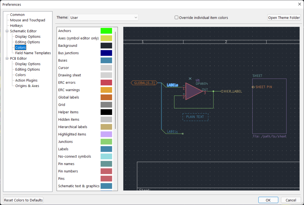
Themes define how things appear on your screen with what colors. Themes are important because you will have to stare at your screen for hours to design a schematic or PCB. The colors should not strain your eyes if you have to work comfortably. For this reason, dark themes are used to reduce the amount of light reaching your eyes and thereby reduce the strain. Themes are now a standard feature in KiCad version 6 and you can customize them as you wish. You can also create new themes and save them as JSON files. These JSON files can be shared with your friends and they can simply copy and paste them to the theme folder to use it.
KiCad v6 comes with a light theme for the schematic and a dark theme for the PCB editor. But we use a dark theme for both schematic and PCB. The themes we use are less contrasty and use more comfortable colors than the contrasty red and blue. See some of the screenshots.
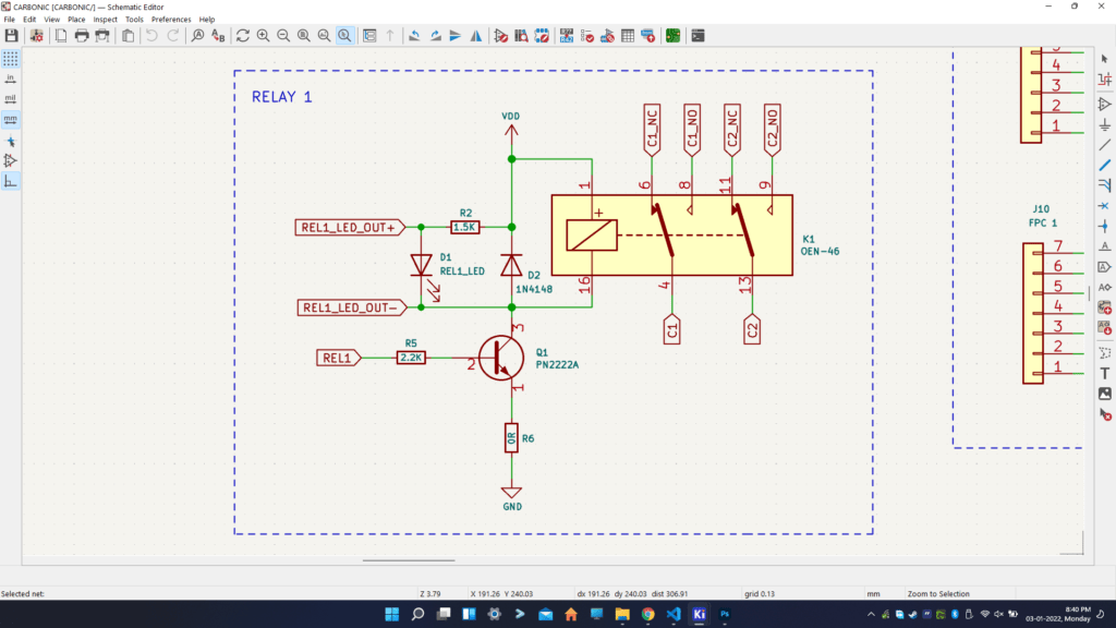
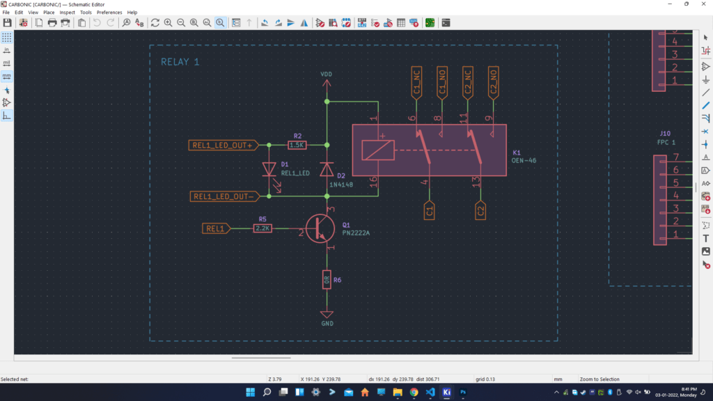
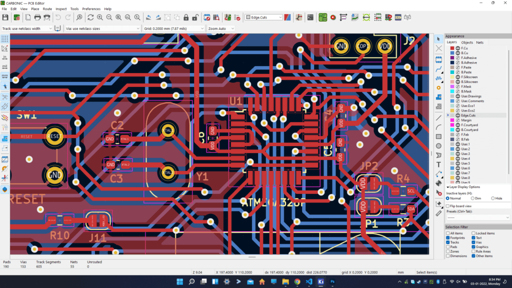
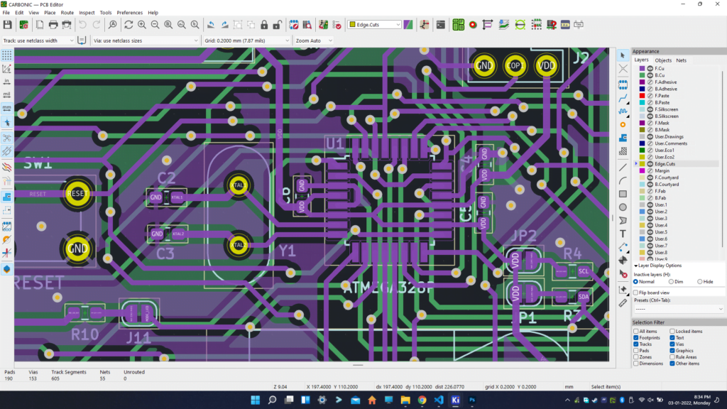
You can install more themes from the PCM. If you have better themes, feel free to share them with us. You can access the theme settings from Preferences → Schematic Editor → Colors.
Keyboard Shortcuts
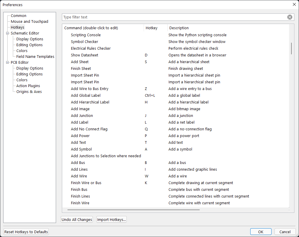
Keyboard shortcuts can make working with KiCad much faster. Most of the functions of KiCad can be mapped to some keyboard shortcut and can be individually set for schematic editor and PCB editor. The most important and common shortcuts are,
- M – Hover on any items and press M key once to select and move it when you move your mouse. This is an absolute move that breaks any connections made to that component. There are other ways to move things without breaking connections.
- C – Hover on any item and press C key once to create a copy of it.
- W – Pressing once selects the Wire tool with which you can interconnect components.
- G – To move items without breaking connections. This operation is called Drag.
- D – Pressing once after hovering on a component opens the datasheet (if it is specified in the symbol) in a browser.
- E – Open the properties window of any item.
- R – Rotate an item. Pressing this again and again rotates the item consecutively.
- X – To mirror an item in the X direction.
- Y – To mirror an item in the Y direction.
- F (in PCB editor) – To change which side an item is.
- V (in PCB editor) – To place a via while the routing tool is active.
- Ctrl + Left Click (in PCB editor) – Highlights the net.
- Shift + U (in PCB editor) – Pressing this each time when a track segment is selected causes each of the remaining sections of the track to be also selected (chain selection). This is the easiest way to select long and segmented tracks when you want to change the track thickness or delete it entirely.
- Shift + S – This is a shortcut we use to switch between schematic and PCB editor. Doing this otherwise is a little slow due to the fact that the buttons to switch editors are not situated at the same place on both editors.
There are so many other shortcuts and you can customize them by going to the Hotkeys section of the preferences.
Schematic Editor
Schematic editor helps you draw the actual circuit diagram. Each component such as resistor and capacitor has unique graphical representations called schematic symbols. You can place these symbols on a drawing sheet and connect them with wires. Each symbol will have pins to which you can attach these wires. We will now explain all the general aspects of drawing schematics. This applies to any EDA tool regardless of how the interface looks. First, let’s create our first KiCad project and explain each aspect in detail.
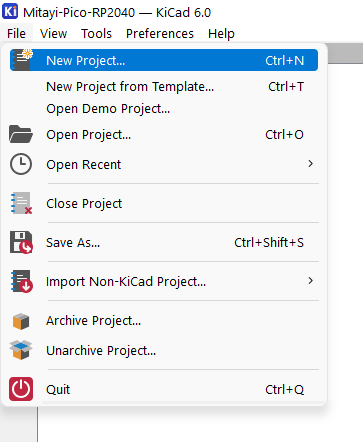
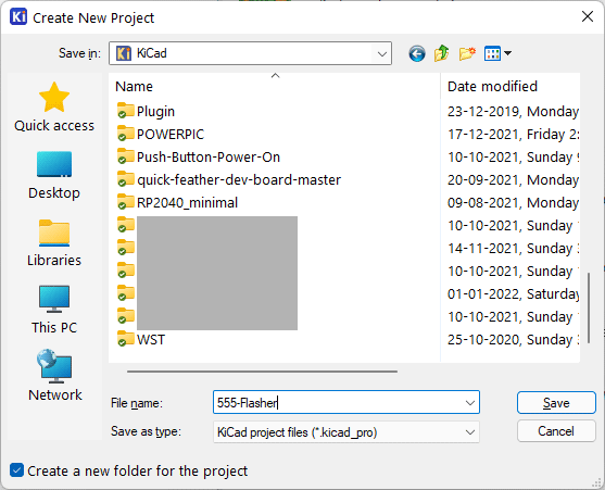
Open the KiCad application. You will see the dashboard with a list of applications and the last project you opened if there are any. Create a new project by going to File → New Project and save the project somewhere. KiCad will automatically create a project folder at the location you selected. You can also override this feature. We are creating a new project called 555-Flasher.
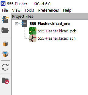
As soon as you create a project, three files will be created in the project folder; KiCad project file (.kicad_pro), a schematic file (.kicad_sch) and a PCB file (.kicad_pcb). Now double click the schematic file to open it. You will see an empty drawing sheet as seen below. The default paper size is A4.
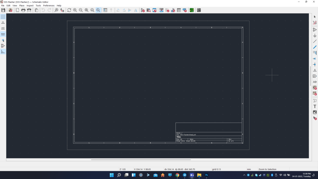
On the left pane, we have a set of appearance control functions. On the top are the process buttons and on the right are the tools to accomplish different tasks such as adding new symbols. On the bottom is an information pane, which shows, from left, the currently opened file name, zoom level (or scale), XY coordinates of the mouse pointer, the difference in XY coordinates from a reference point (delta values), grid size, currently selected unit and the currently selected tool name. These values will also change when you select an item.
Worksheets
Worksheets are equivalent to paper sheets where you have to draw the schematic/PCB. While in reality, we can only draw within the limits of the paper, in KiCad we can also draw outside of it. But this does not necessarily mean you should. We use worksheets to keep the schematic organized and it becomes important when the schematic is large and you have to use multiple sheets. And yes, a KiCad schematic can contain multiple interconnected sheets. You can customize the names of each sheet and add other details.
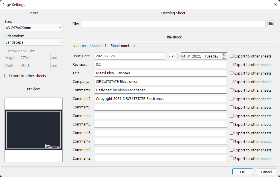
When you open KiCad’s schematic editor you will see an empty sheet. You can change the sheet size and orientation by going to File → Page Settings. A drawing sheet has borders that are numbered and on the bottom right will be a title block. You can hover on this title block and press E to open the sheet properties. If you want to add a new type of sheet and want to save it for future designs, you can add them using the Drawing Sheet Editor tool as we discussed before.
Grid
The second thing you will notice is the grid; evenly placed small dots. The grid is where all items on the schematic will snap to by default. The mouse pointer will also snap to grid points when you move it. You can see this in action by zooming in and seeing the mouse pointer always move at specific lengths in all directions. Every schematic symbol, wire, and text will be snapped to this grid when you place them. The grid is important because if you change the grid, you will no longer be able to snap to the pins of schematic symbols. This could happen when you accidentally press hotkeys to change the grid and continue to add more symbols without realizing it. The keyboard shortcut to change the grid to the next size is N. You could press this accidentally and change the grid. This is a mistake beginners usually make. But do not worry. When an item is not aligned to the current grid, you can simply select one or more items, right-click, and choose the Align Elements to Grid option from the menu. This will realign all items to the current grid.
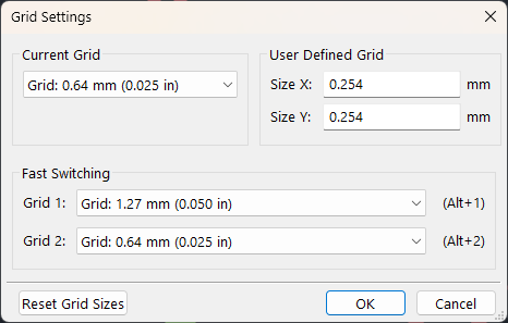
It is better to keep the grid to the default value of 0.64 mm (minor grid), and 1.27 mm (major grid) You can change the grid size by right-clicking on any empty area on the sheet. You can hide the grid by pressing the grid button on the left pane. You can also change the grid unit to mm, mil, and inch. It is recommended to keep it in mm.
The bottom information pane will show the XY coordinates in the grid. This grid also has an origin point located at the top left corner of the sheet. If you move your mouse pointer to this point, the XY coordinates will become 0. This is the default origin point or zero point used for everything on your schematic and PCB.
Units
We use mixed units for electronic design. For example, the pitch (distance between each pin) of a standard Dual-in-Line (DIP) package is 0.1 inch. Your breadboard also has this pitch. But we no longer use inch (or other imperial units) but we also can not change established values since it is already been used for too long. The solution is to convert all inch values to their closest SI unit values. 0.1″ is converted to 2.54 mm. So whenever you see any connector or pins having a 2.54 mm pitch, that means the component will also align with your 0.1″ pitch breadboards. You just have to keep these conventions in mind when working with any CAD. Try to always use millimeters and explicitly specify them whenever you can.
Another commonly used unit in the PCB industry is the mil. A mil is a thousandth of an inch. PCB manufacturers usually specify track widths and clearances in mils. You just have to know that 1 mil = 0.0254 mm.
Schematic Symbols
As we said before, schematic symbols are graphical representations of actual components. The schematic symbol is designed in a way that all the pins of the component are exposed so that we can connect other components to it. Pins can be numbered as per the datasheet and also be grouped depending on their functions. Additionally, other markings and symbols can also be added to the schematic. Below is a schematic symbol of an NPN transistor.

Observe how the Emitter pin is marked with an outgoing arrow. For a PNP transistor, this will be in the opposite direction. You can also see the numbering of pins. The symbol has two additional parts. The one in purple is the reference designator. Q? means it is a transistor with an undefined reference number. That is how we number parts on a schematic. We could have more than one part in our schematic. It then becomes important to number them in some order. Reference designators usually consist of letters and a sequence number. There are no standards but there is a consensus over which letters are used for which type of part. Following is a list of widely used reference designator letters.
R– ResistorC– CapacitorL– InductorU– Integrated CircuitsK– RelayD– DiodeQ– TransistorJ– ConnectorsY– CrystalsSW– SwitchJP– Jumper
The reason why the ? appears after the reference designator is because we have to yet annotate our schematic. In other words, we have not finalized the schematic yet. We can add sequence numbers to the reference designators, only after we finalize the schematic. After annotating, the reference designator can change to Q3, for example. We will come to that further down in this tutorial.
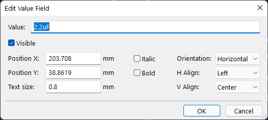
The second part in light green is the value of the component. For example, this could be 100 Ohms for a resistor. Understand the difference between a component value and a reference designator. Two different resistors can have the same value but not the same reference designator. You can change the value by hovering on the text item and pressing the key E once. Usually, this value will be defined in the schematic itself.
Power Symbols
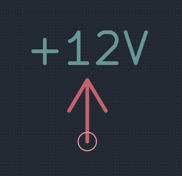
Not all symbols you see on a schematic correspond to actual components. Power symbols are of this kind. They are used to interconnect common points together but without a creating mess of interconnecting wires. Parts of your schematic where these symbols are placed get connected together even if there are no wires directly connecting them. Common power symbols include positive supply rails, ground, earth, etc. Power symbols also do not have reference designators since they are not actual components. They only have values such as +12V which you can not change. Power symbols can be placed using Add power port option on the right pane. The shortcut is P. We will see how we can use these symbols in an example later.
SPICE Symbols
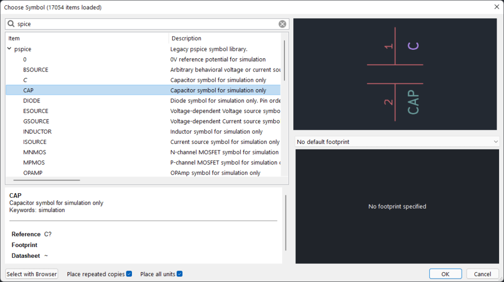
Another type of symbol is called simulation primitives. As we have explained before, KiCad also supports popular simulation engines such as SPICE. For simulating a circuit and analyzing its performance under various conditions, we have to use the simulation primitives; symbols that are only used for simulation. These symbols also have reference designators and values. But they can never be assigned with a footprint and used in a PCB design. We won’t be covering the simulation tutorial here but we will show it in a different post later. For now, just keep in mind the simulation-only symbols. Make sure you don’t use them in a normal schematic.
Symbol Libraries
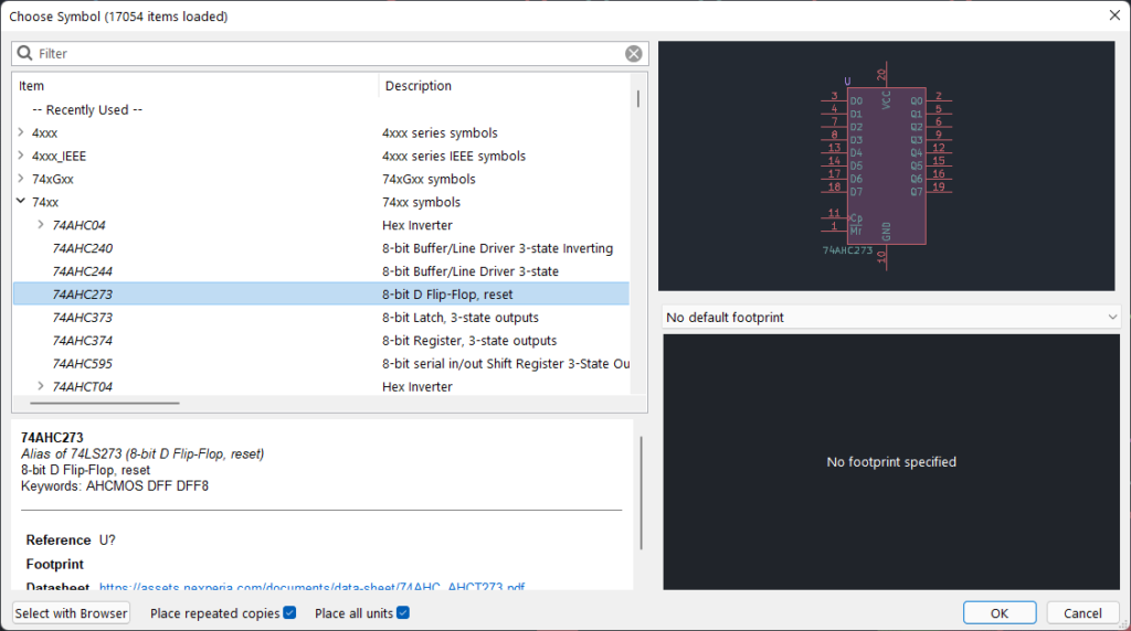
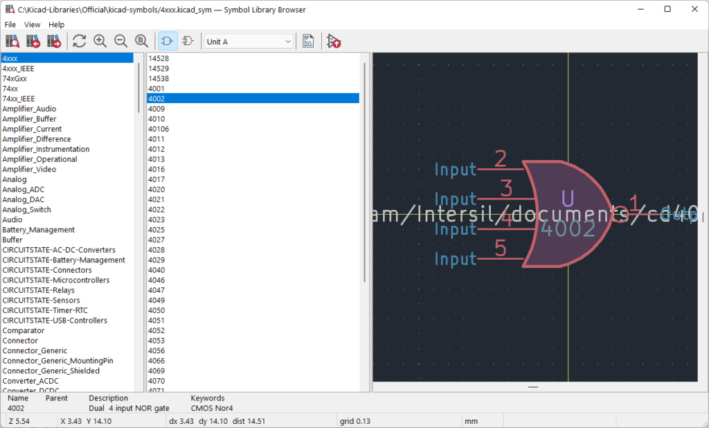
There can be thousands of unique components and thousands of schematic symbols will be needed to represent them. When things are high in number, we can organize them according to their similarities. Schematic symbols are also categorized this way, into similar groups. For example, all 7400 series logic ICs can be grouped together since they are a single family of chips. Such collections of symbols are called symbol libraries. Each library can have hundreds of unique components. You could also create a new symbol and add it to this library to expand it. In KiCad, symbol libraries can be opened using the Add a symbol tool. You will be able to see all currently available symbol libraries. You can also open them from Browse symbol libraries option on top.
Drawing Schematic
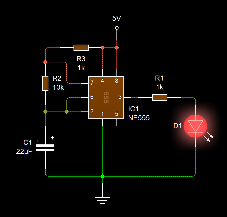
Now that we have explained the basic concepts, we can start drawing a schematic. This way, you can learn about what tools to be used when, and the general workflow. We will use the following simple 555 Flasher circuit as our reference. The circuit diagram was created using Circuit Wizard.
First, create a new KiCad project called 555-Flasher and save it somewhere on your computer. It will be better if you save it to a common KiCad project folder so that you can access all projects from one place. Double click on the schematic file to open it. You will see the empty worksheet. Scrolling, panning, and zooming on the worksheet are accomplished with the help of a mouse.
- Zooming in and out – just use the mouse scroll wheel to zoom in and out.
- Panning – click and hold the center mouse wheel button and move your mouse.
- Scrolling – press Shift and scroll the mouse wheel for vertical scrolling and press Ctrl and scroll the mouse wheel for horizontal scrolling.
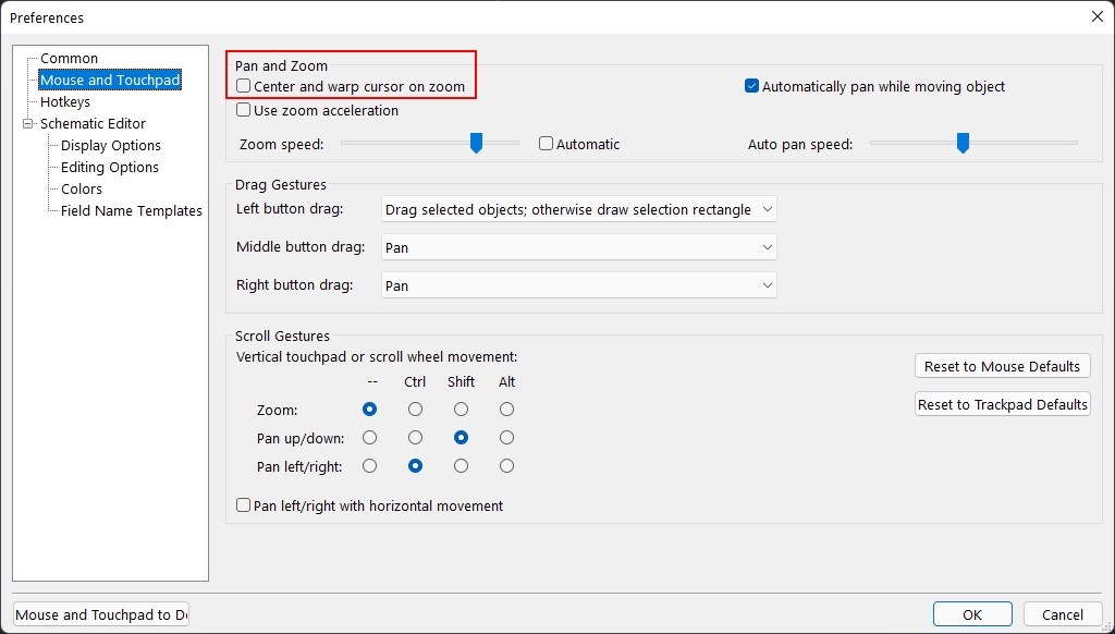
Whenever you zoom, the mouse pointer will automatically move to the center of your work area. This is the default behavior and you might not like it; we don’t. You can change this by going to the Preferences → Mouse and Touchpad settings. Uncheck the Center and wrap cursor on zoom option.
The first step is to place all the symbols we need. To do that, find the Add a symbol button from the right tool panel. You can also press A key on the keyboard. This will open the Choose a Symbol window. In the filter box, just type “555” to easily find the part we are looking for. In this case, we want NE555 in DIP-8 package. You can see we have selected and highlighted that part from the Timer list.
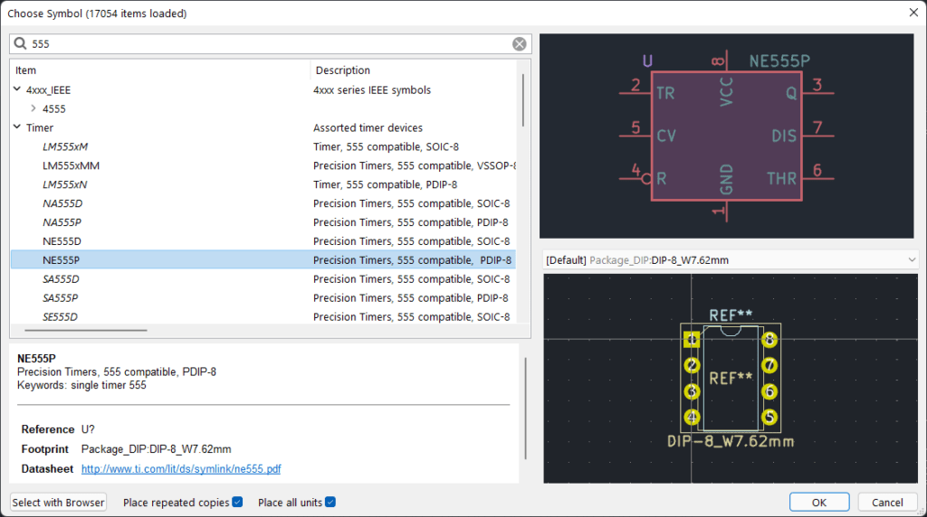
The interface can be a little different for you. That is because we have turned on the Show footprint previews in Symbol Chooser option from Schematic Editor → Editing Options settings. This will also show the default footprint associated with the symbol we are selecting. If there are no footprints associated with a symbol, nothing will be shown. It is okay if that’s the case because we can always assign a new footprint to a symbol.
Once you have selected a symbol, double-click on the item to place it. Or you can also click the OK button. This will now show your mouse pointer attached with the new symbol. Click anywhere on the worksheet to release the symbol. If you had the Place repeated copies option turned on, a new symbol will appear on your mouse pointer just after placing the first one. This can be handy if you want to place multiple symbols. But we can also Duplicate a symbol anytime we want. Now we have to choose the resistor. Open the symbol chooser again and search for “resistor”. From the list, choose R_Small. This is a smaller version of the standard size resistor (R). We use the smaller versions to save space and keep the schematic compact. If you prefer the zig-zag type symbol, choose the US versions (R_Small_US) of the symbol.
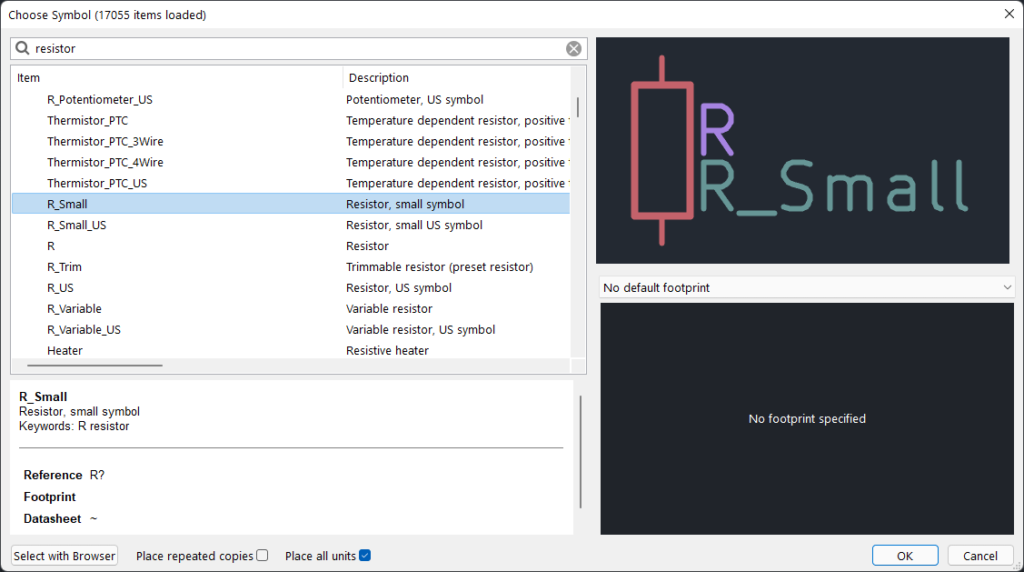
Since there is no default footprint associated with the resistor symbol, there is no footprint shown in the preview window. We just need to place only one symbol even if we wanted more because again, we can duplicate the symbols once we have placed them on the sheet. So let’s choose the C_Polarized_Small for the capacitor. For LED, just search for “LED” and choose the LED symbol.
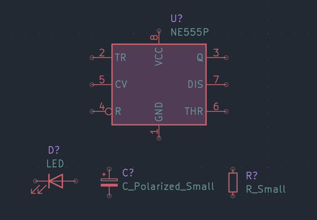
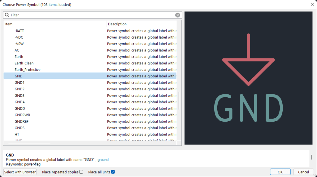
That will be all the part symbols we need. But we also need the power symbols to show where the power supply lines are connected to. For that, first, dismiss the Choose Symbol window by pressing Cancel or pressing Esc button on the keyboard. To choose the power symbols, find the Add a power port button from the right tool panel. You can also press P key. This will open a window similar to one we have seen before. From under the power category, find the +5V symbol and place it on the schematic sheet. We also need the GND symbol for the negative line. That can be found under the same category. Place one GND symbol on the sheet, then close the window. Now we have everything for creating the schematic.
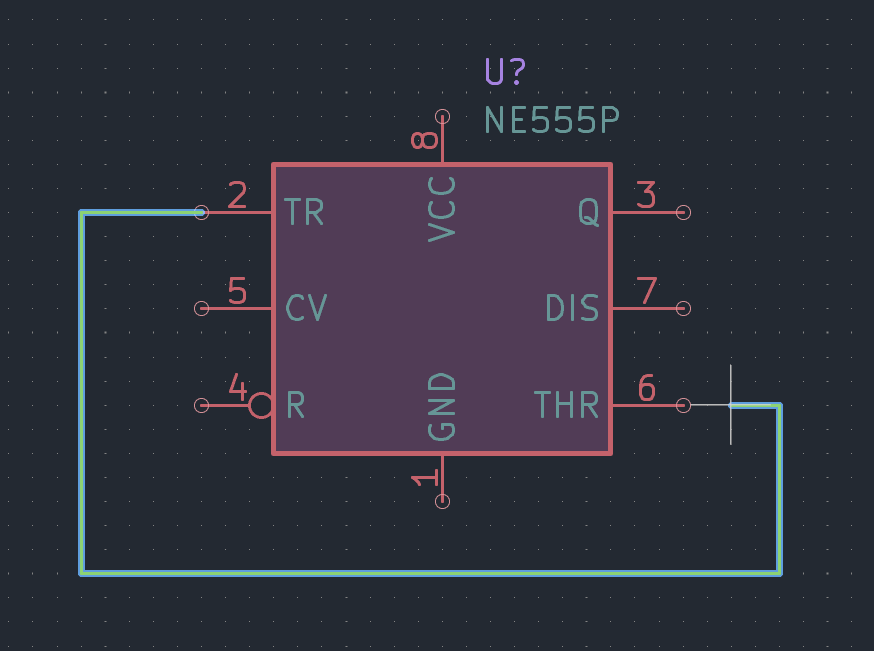
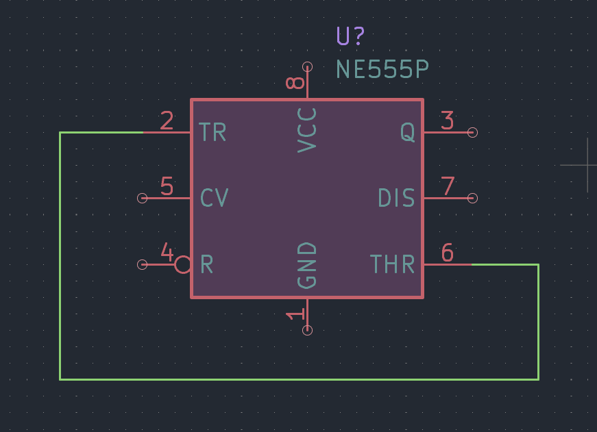
Once we have all the symbols, we can start interconnecting them. First place the 555 symbol around the center of the sheet. Move other symbols to the side, by selecting them all and pressing M key to move. Let’s first connect pins 2 and 6 as per our reference circuit diagram. But you will notice that the sides where pins are arranged on the symbol are different from the KiCad symbol. On the reference circuit, these pins appear to be closer and thus easy to interconnect. If you feel like you want to make a better symbol for 555, that is when we can use the Symbol Editor tool. But we will do that later on in a different post. For now, let’s work with what we have.
To connect pins 2 and 6, choose the Add a wire tool from the tool panel or press W. Then zoom into the schematic where pin 2 is and click on the end of the pin, where a circle appears. Now you have a wire coming out of the pin which you can terminate elsewhere.
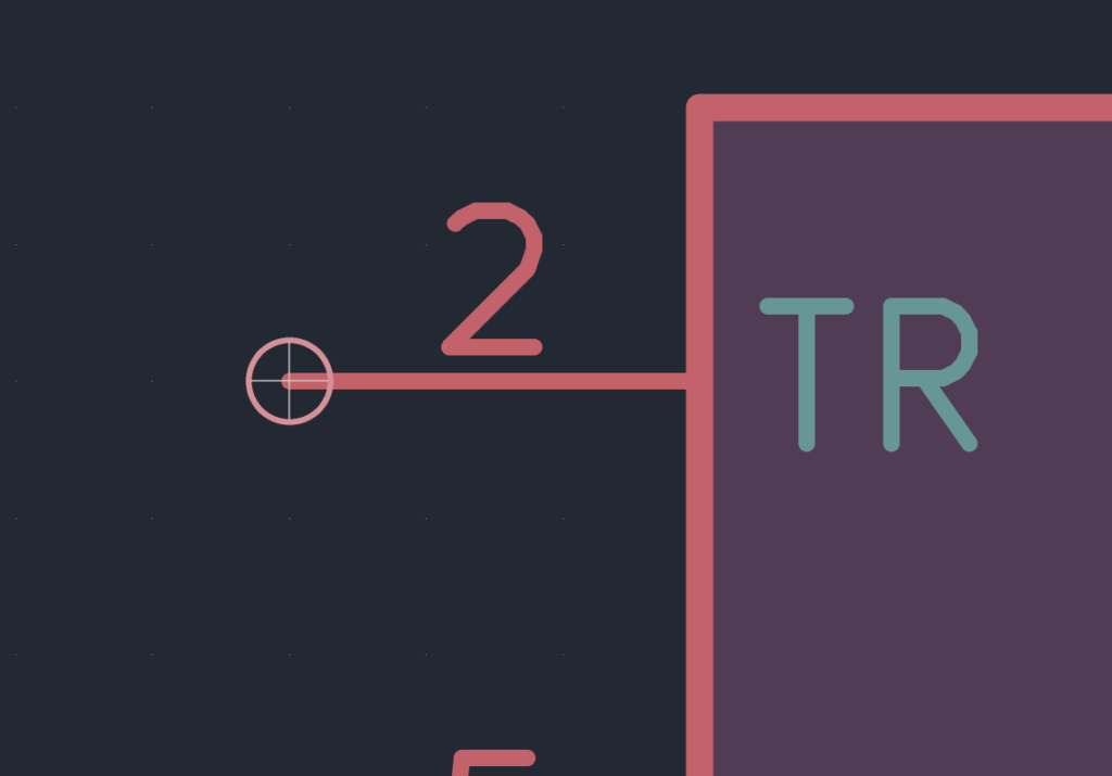
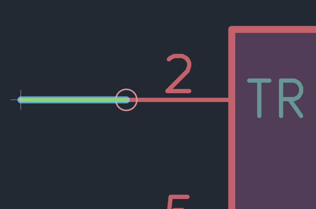
We have to terminate the wire at pin 6. For that, zoom out and guide the wire around the bottom of the 555 symbol. When you want to change the direction of the wire, you can click once to place a new corner and continue drawing the wire from there. You can always terminate the wire by double-clicking or right-clicking and choosing Finish Wire option. Pressing Esc key once when the wire tool is active will cancel the whole operation. Since we want to connect pins 2 and 6, bring the other end of the wire to pin 6 and left-click once. This will automatically terminate the wire and now we have an interconnection.
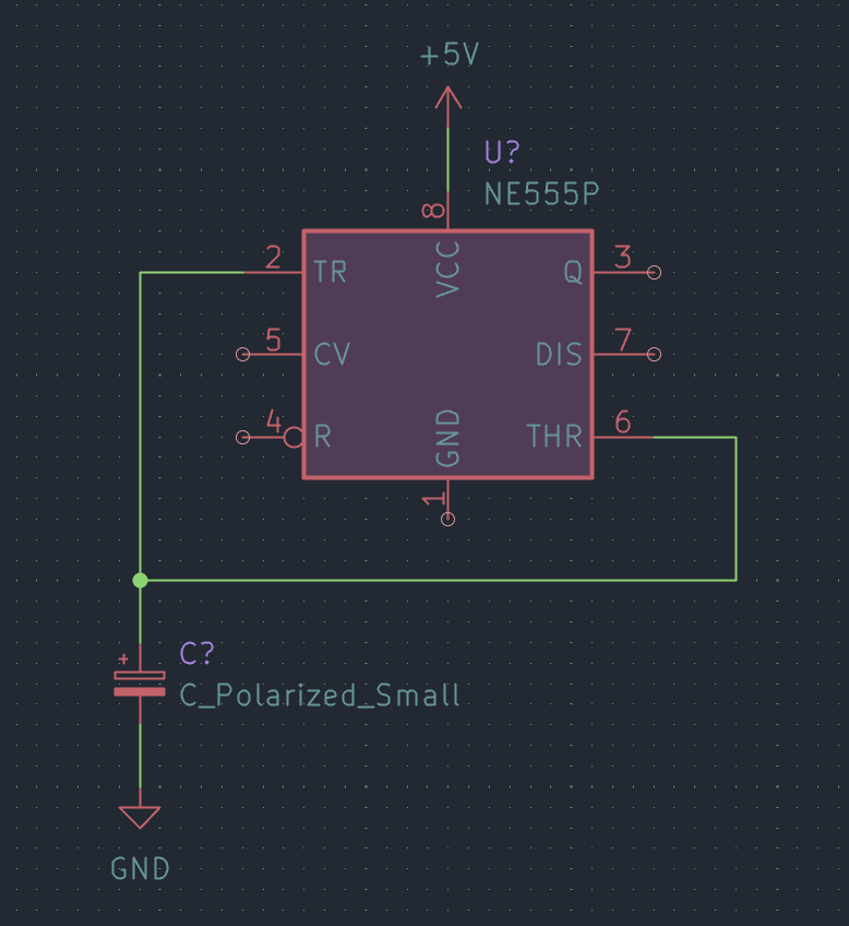
Now place the capacitor and power symbols as shown below and connect them. When you connect wires together, the point they meet will automatically create a junction represented by a dot. A junction can also be placed manually with the Add a junction tool or pressing J.
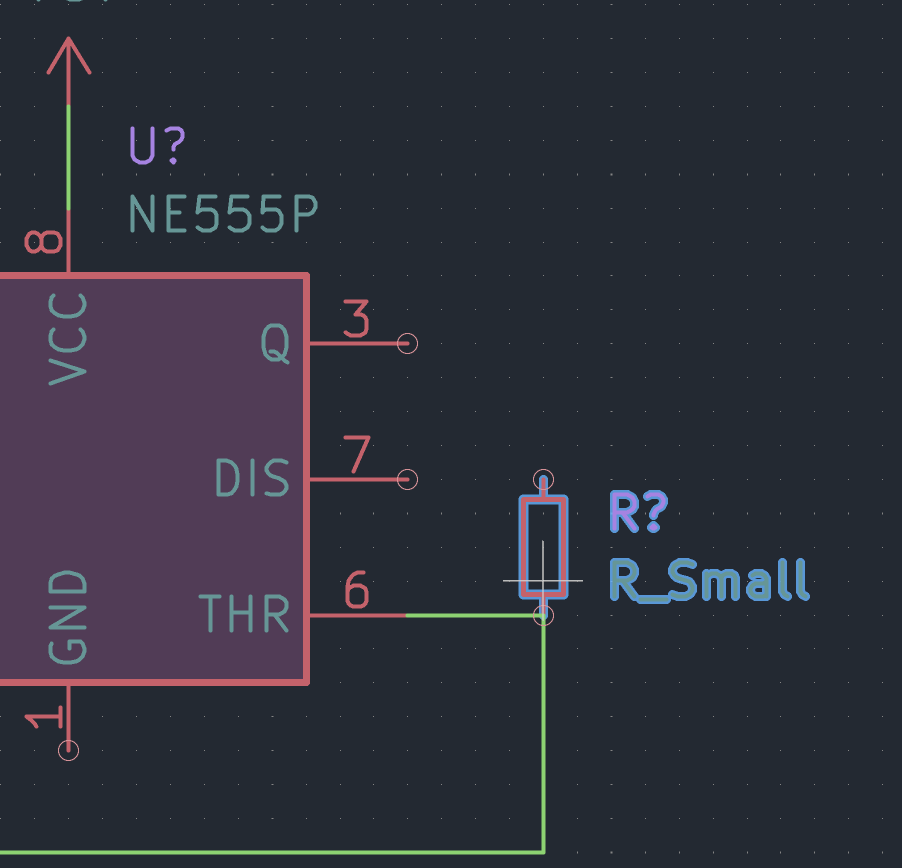
Now bring the resistor symbol closer to pins 7 and 6 and connect them. If the symbol is in the wrong orientation, you can press R key to rotate it. You can also press X and Y keys to mirror symbols.
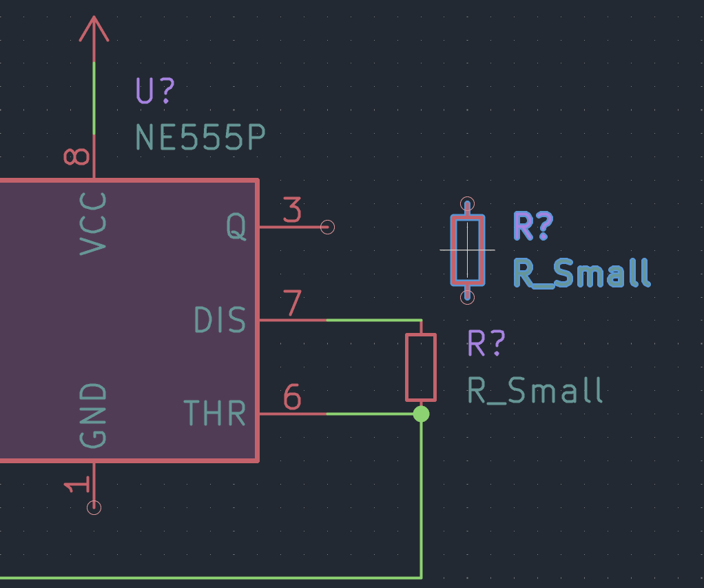
The advantage of using smaller versions of symbols is that you can arrange them in compact spaces. Now we need one more resistor. Instead of placing one from the symbol library, we can simply duplicate a symbol that is already on the sheet. Hover over the resistor symbol and press D key once. This will create a copy of the symbol and you can place it anywhere. Place it horizontal to pin 7 and connect them.
After placing the resistor, we want to connect the other end to the positive rail. You might think of doing something like the below.
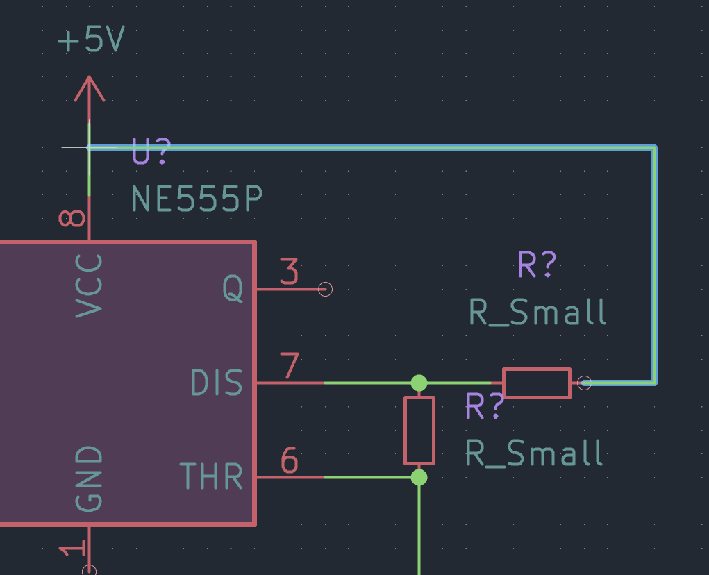
But observe closer; we have pin 3 to which we want to connect an LED and resistor. So the new wire you will be placing is going to be around them and it can limit the space there. Not only that, the schematic can look confusing at first look. So let’s not add a wire like that. Instead, we will just duplicate the +5V power symbol and place it near the resistor and connect them.
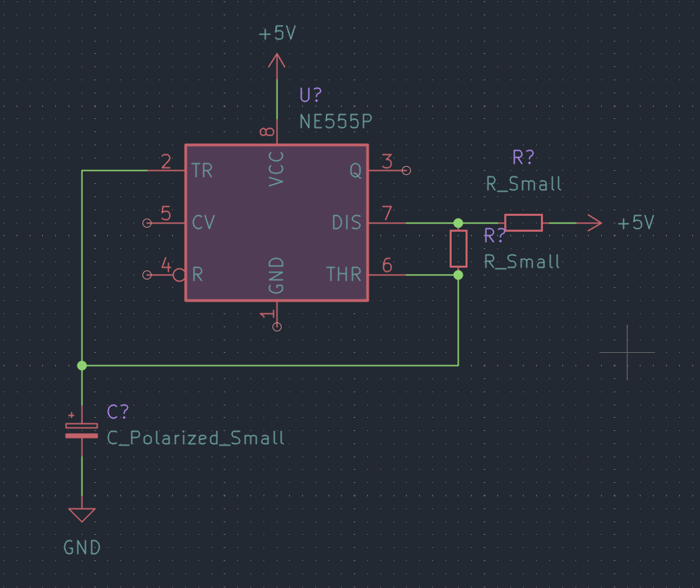
Now the resistor is connected to the common +5V rail even though there are no wires connecting them. That is neater right? You can duplicate the power symbols any number of times because they are not actual components. Something else you might be thinking about is the text size. You would wish if the text size was a little smaller so that they don’t overlap with the wires and symbols. You can move the text fields anywhere you like using M key. But if you want to change the text size, you can click on the item and press E key once to open the properties. You can also double-click on the item. Changing a few text sizes would be fine with this method. But what if you have so much text you want to change the size of? For that, we can use Edit → Edit Text & Graphics Properties menu. Open the window and set the options to exactly what shown below. For the text size, enter 0.8 and then press OK.
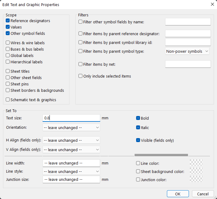
Now all the reference designators and value fields will have 0.8 mm size, much more compact.
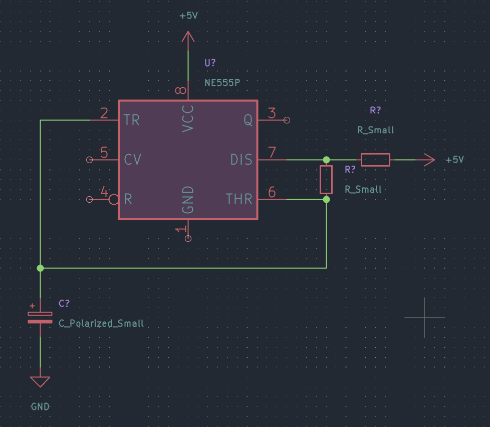
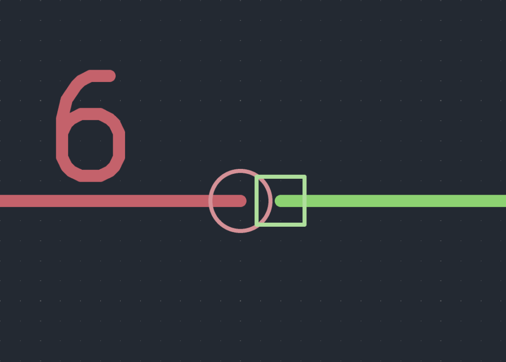
Let’s proceed to finish the schematic. Place all symbols and connect them. Make sure you terminate all wires properly. An improperly terminated wire will show a square box at the end of it.
Once you finish the schematic, it will look something like this.
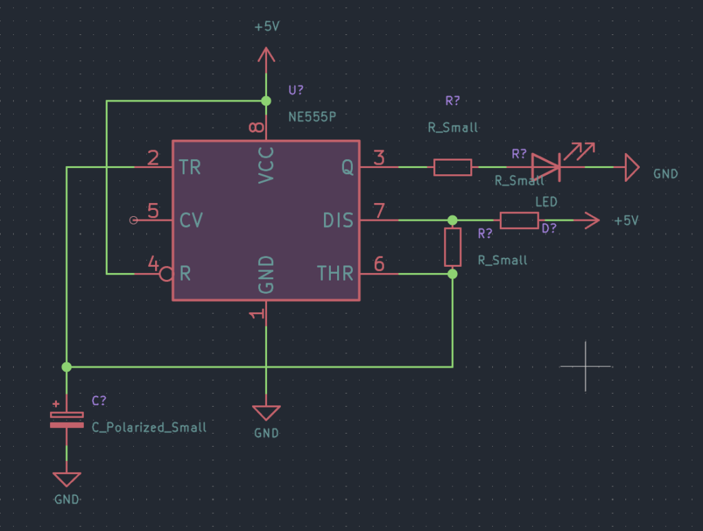
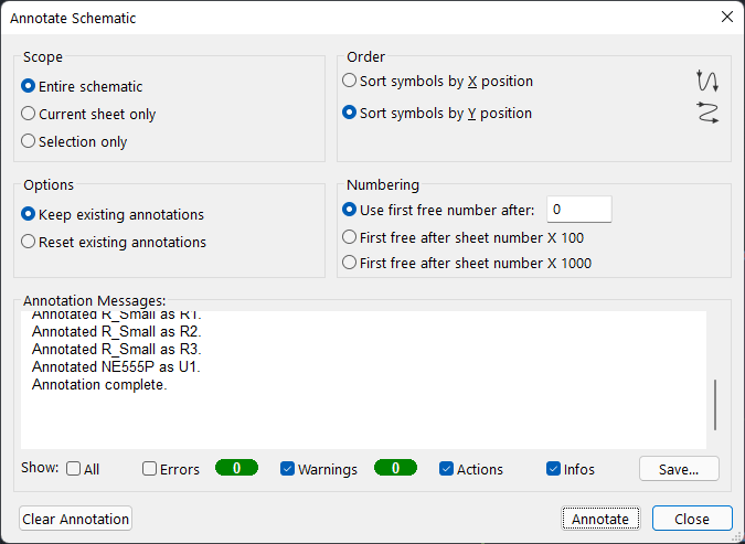
We still have not annotated the schematic. Annotation is the process of adding sequence numbers to symbols. We can do this by going to Tools → Annotate Schematic. Keep all options as below and click OK.
You will now get an annotated schematic as below.
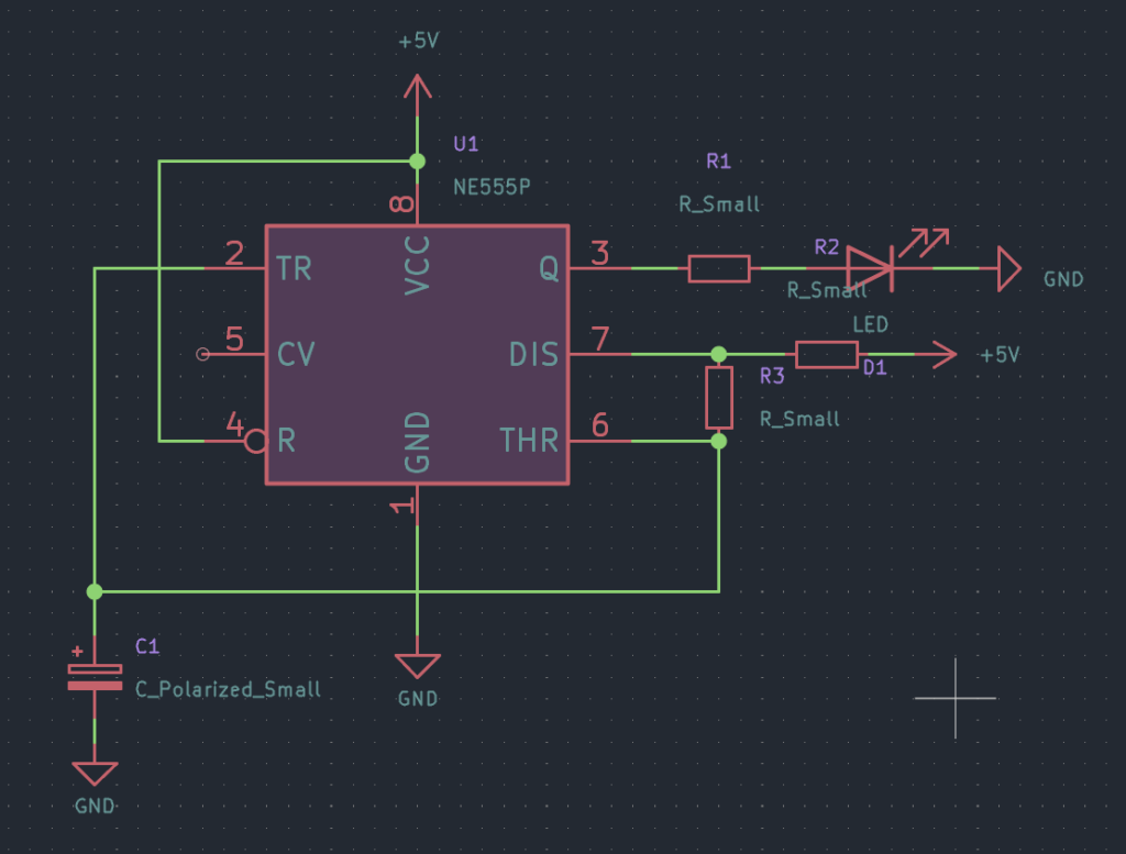
We still don’t have values for the components. To add values, just double-click on the value text and enter a new value.
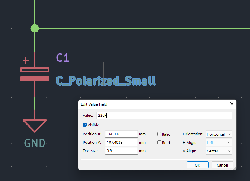
Once we added all the values, the schematic will be almost complete. We also have arranged the text neatly.
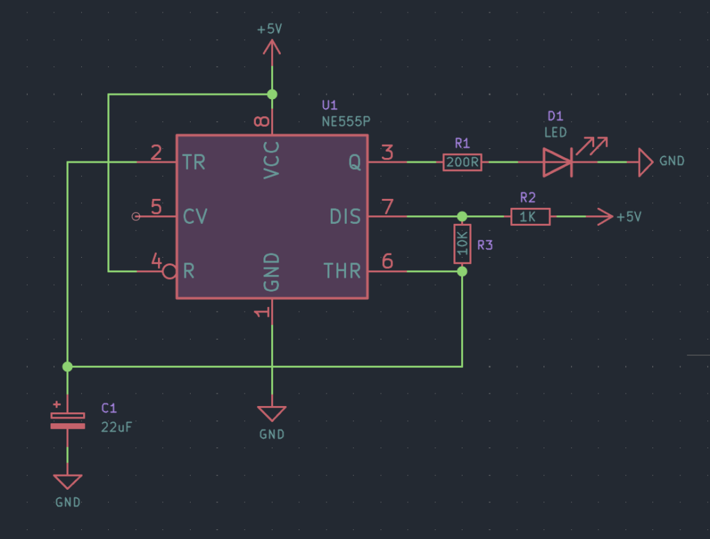
There is one more tiny thing to do. See that pin 5 floating and connected to nowhere? When pins of a symbol are not connected anywhere, we can explicitly tell KiCad that they are not connected. This is important at a later stage when we run the Electrical Rules Checker (ERC). The ERC will complain about unconnected pins. This is a good thing because if we ever forget to connect an important pin, or the wire was not properly connected, the software can tell us about it. To show that a pin is not connected, we can place the no-connection flag using Add a no-connection flag option.
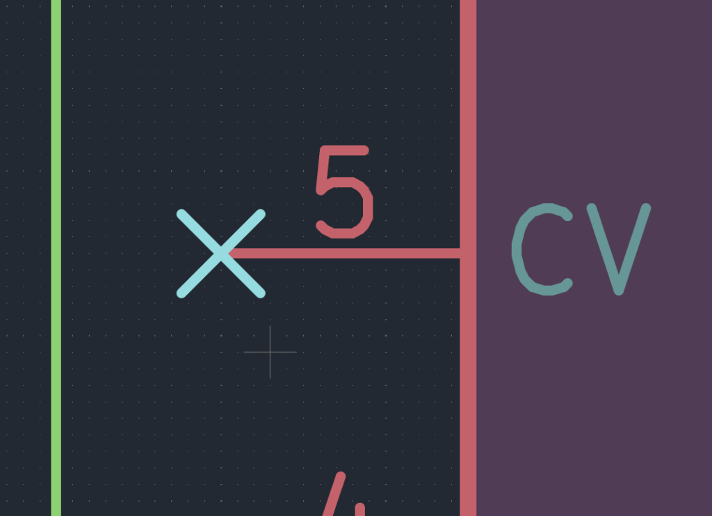
Now that we have completed the schematic, let’s talk about annotations in detail because that is an important aspect when drawing a schematic.
Annotation
You must have noticed that whenever we place a new symbol, their reference designators have a ? at the end. We have explained why. So how do we get the sequence numbers then? Once you have completed the circuit and you are confident everything is right, you can start numbering each type of component. This process is called annotation. To annotate your schematic, simply go to Tools → Annotate Schematic or click the respective icon on the top bar. This will open up a new window with a few options. You can specify which items you want to annotate, the order, whether to keep already existing annotations, and the starting number of the sequence. Once this process is complete, all your symbols will have unique reference designators.
But what happens if you removed a component? If you remove a component from an annotated schematic, that sequence number will be freed and could be assigned to another symbol. For example, say you had 10 resistors in your schematic. When you annotate them, each resistor will get reference designators like R1, R2 to R10. Now if you removed R4 from the schematic and added two new ones, the total number of resistors has now increased to 11. The newly added resistors do not have annotations yet. You have two options in this case.
- Remove all existing annotations and reannotate the entire schematic. This can cause existing components to lose their previously assigned numbers. This can become really confusing and mess up so many things, because the resistor you called
R3could becomeR8now, or anything else. - Keep all existing annotations and add new ones. When you do this, you will get 11 resistors numbered from
R1toR12. WhyR12is because we are keeping previously assigned numbers. SinceR4has been deleted, that will also be kept. The reannotation will start from 11 after theR10.
Electrical Rules Checker (ERC)
A schematic can have hundreds of symbols and much more interconnections. How do we make sure everything we have done is right? What if we missed something? The software can help us identify potential issues with the schematic, only if we specify the rules. For example, say you accidentally connected a positive supply rail to GND which is a catastrophic mistake. If we specify that certain pins are power only and opposite polarities should not be connected, the software can check the entire schematic if any part of it violates that rule. This process of automatic checking of electrical rules is called Electrical Rules Checker or ERC.
Electrical rules and their severity can be configured by going to File → Schematic Setup menu. ERC is a little complicated matter and therefore we won’t be explaining it in detail now. But let’s run the ERC for the schematic we just designed and see what the ERC says. Run the ERC from Inspect → Electrical Rules Checker. This will open a new window and press the Run ERC button there.
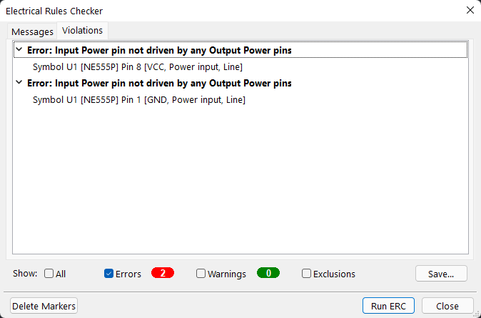
We just found two errors. When you click on each error, the part of the schematic where the error is will be highlighted along with an arrow.
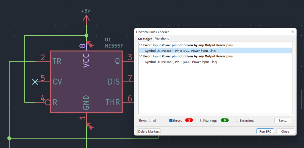
So what are the errors? The ERC is complaining about not being able to determine where the power is coming from. When we design a schematic symbol, we have the option to choose what types of pins it has. This can be input, output, power, etc. The NE555P symbol we used has its pins defined this way. The VCC and GND are power pins. If such power pins are present, they must be connected to a power source that has a power output pin. This can be some other symbol, such as a battery. Since we don’t have such a source in the schematic, the ERC assumes that the VCC and GND pins of NE555P are not connected to any sources. To bypass this error, we can tell the ERC that our schematic does not have a power source and all the pins themselves are powered. For this, we have to use a special symbol called the Power Flag. It can be placed using Add a power port option. Since we have two power pins in NE555P, we have to place one power flag on the VCC line and one on the GND line.
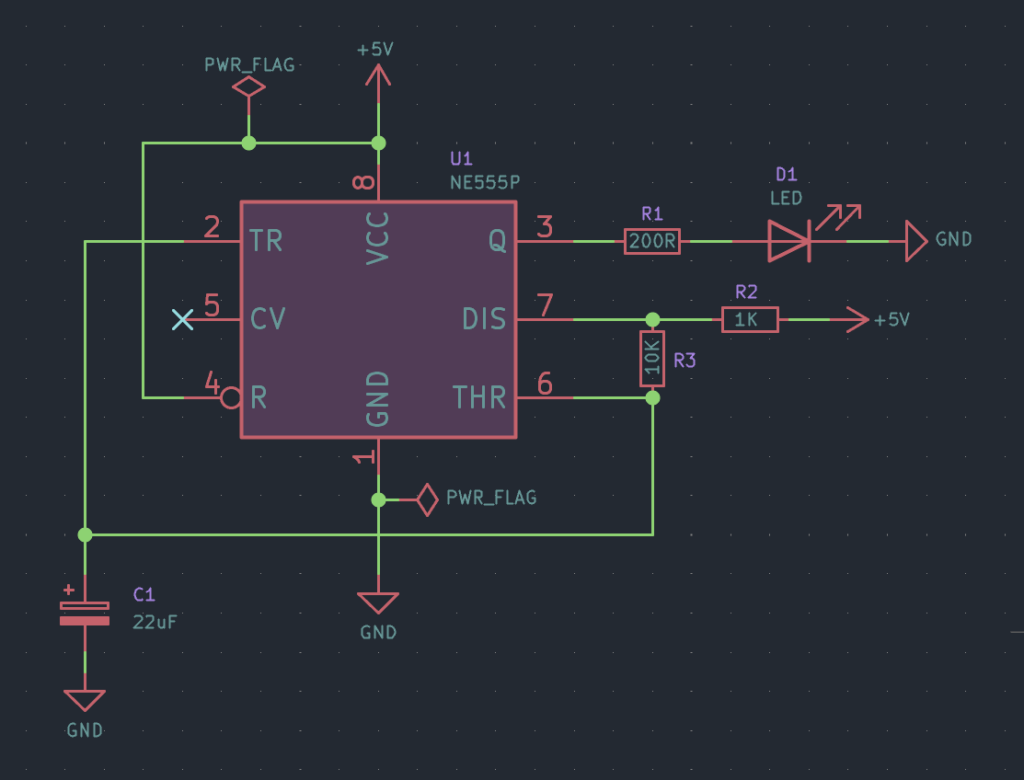
Remember that adding the same power flags to both +5V and GND lines does not mean they get connected together. The power flag’s only job is to tell the ERC where power is at; nothing more. Now run the ERC again and you will get zero errors.
Labels
We have seen how we can use power symbols at multiple locations to connect signals together without using long wires. The same functionality is available in KiCad as Labels. Labels are custom-named flags that can be connected to any wire or pins. Labels can be duplicated any number of times and labels of the same name connects all nets together. It keeps the schematic simple and neat.
There are three types of labels in KiCad; Local, Global, and Hierarchical. A local netlabel only applies to the local schematic sheet only. Use the Add a net label icon or press L to place a new label. Type a name and other properties and press OK. Now you can place the label anywhere on the sheet. It will have a pin at one end where you can connect a wire. You can duplicate the label and place it somewhere else when you want.
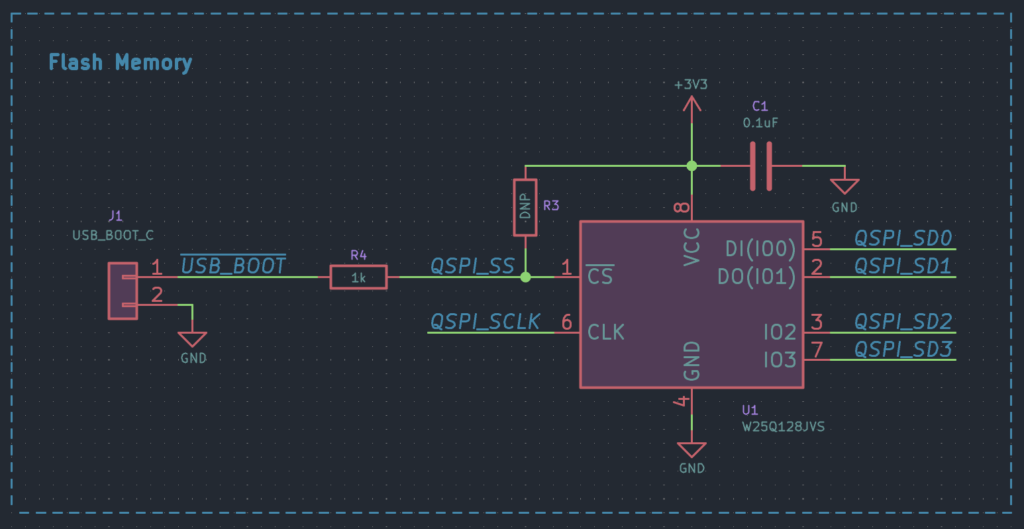
Now, why is this called a local net label? You can think of them as local variables in a programming language. A local variable only applies to a particular context where it is defined. Another context or a function can have a local variable of the same name but a different value. Similarly, local net labels only apply to the schematic sheet they are currently placed in. You can have the same net label on a different sheet (KiCad supports schematic with multiple sheets btw) but they will not be connected together. This helps us to reuse net names and abstract complex schematics in a better way.
Global labels are similar to global variables. They apply to all sheets within the project. You can add a global label using Add a global label button or press Ctrl + L. The global label has a distinctive look that can be customized. Once placed, use the pin to connect to a net. Any that is connected to this label will be considered as a single net.
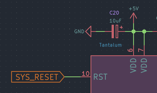
Yet another type of label is called a hierarchical label. As we said earlier, we can use local net labels within a sheet. But sometimes we want to expose some nets from one sheet to other sheets. This can be done using global labels of course, but we will lose the flexibility in abstraction. Hierarchical labels help us to expose some of the nets to the outside scope so that other sheets with their own set of hierarchical labels can connect to each other.

Netlist
A schematic diagram is a graphical representation of electrical/electronic components and their interconnections. But that is not how the software sees it. To the software, it’s all numbers or names. Every pin is a unique point that can be represented in some type of coordinates or numbers. When we connect a pin to another pin using wires, we are creating what is called a net. The same net can have more than two pins connected to it. For example, +5V can be a single net to which all VCC pins are connected. In our schematic, we have pins 8 and 4 of NE555P connected to +5V. We also have one pin of the resistor R2 connected to +5V. This forms a single net. A schematic is a collection of such nets and it is called a netlist. The netlist can be helpful for exporting your schematic to another software, for example, a simulation software. KiCad can also convert schematic and PCB files from other EDA softwares. This is possible because KiCad can read the netlist of the source schematic and convert then to nets used in KiCad. In previous versions of KiCad, we had to manually create and import netlists to create a new PCB. That has changed with version 6. Still, if you need the netlist file for some reason, you can export it from File → Export → Netlist.
Footprint Assignment Tool
Once a schematic drawing is complete in terms of all the aspects we have described so far, we could create a PCB layout from it. Unlike a schematic, a PCB design is a physical or mechanical design where all types of measurements and scales matter. That means, when you work with a PCB editor, you will be limited by the physical/mechanical constraints of the real world. In order to convert the schematic to a PCB, schematic symbols should have their physical equivalents and they are called footprints. Footprints are two-dimensional mechanical layouts where you can solder the actual component. For example, a 5 mm LED needs a footprint with two holes and two pads on the PCB, spaced so that we can insert and solder the LED in place. If the holes were smaller or larger, or placed closer or far apart than needed, we can’t insert the LED without damaging it.
A single resistor symbol you placed on the schematic can have hundreds of types of footprints, because there are resistors of different sizes and shapes. So you need to know what type of resistor you are going to use, prior to creating the PCB. This is what we do with a Footprint Assignment Tool. You can open this from Tools → Assign Footprints.
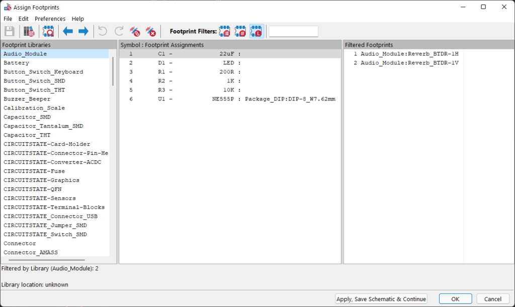
When you open the footprint assignment tool, a new window will appear with three columns. The first column has all the footprint libraries (collections of footprints). Each item on the list is a library and they can have hundreds of individual footprints. We have to find a single footprint from these libraries and assign it to one or more symbols in our schematic. The middle column has our schematic symbols. As you can see, the U1, our only integrated circuit already has a footprint assigned called Package_DIP:DIP-8_W7.62mm. That’s the 8 pin Dual-In-Line package used for NE555 ICs. Let’s break down the whole name and see what each means.
- Package_DIP – this is the library where the footprint is located. If you scroll down the library list, you can see this library on the list.
- DIP-8 – this means an 8 pin Dual-In-Line package.
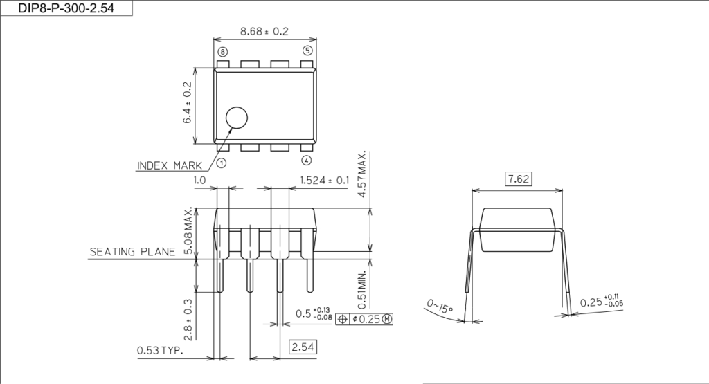
- W7.62mm – this means the width of the IC package is 7.62 mm. The width is specified because there can be other 8 pin DIP packages with different widths.
Have a look at the actual dimensions of this IC package below. Notice the specified width of 7.62 mm (300 mil).
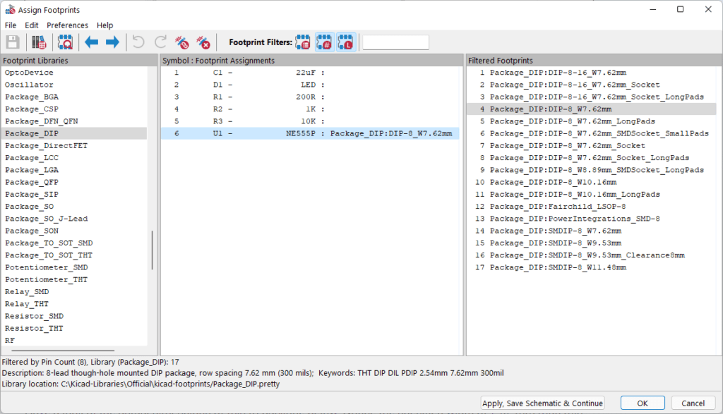
If you highlight the Package_DIP library and the U1 symbol, you can see that the currently assigned footprint is one of the many 8-pin packages, as shown in the third column. This is why you have to be careful with the footprint assignment tool. Choosing the wrong footprint means, that when you get the fabricated PCB in hand, a component might not fit on it. So you have to absolutely make sure that you have selected the right footprints before starting the PCB design.
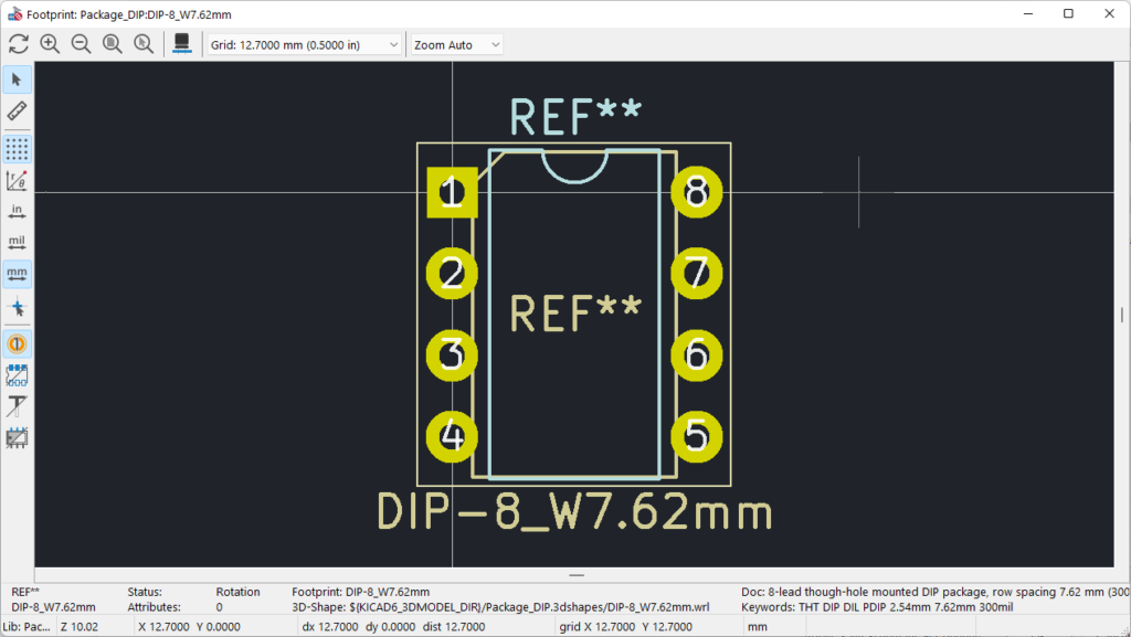
If you want a preview of a footprint, simply right-click on it and open the preview window.
Finding the right footprint from a pool of thousands can be difficult. So to help you with that, the footprint assignment tool has three search filters. These are on the top where it says footprint filters.
- Filter by footprint filters defined in the schematic symbol – When we design a schematic symbol, we can define the footprint filters associated with it. This is to make finding suitable footprints easy. If the selected schematic symbol has such filters defined, turning on this filter will filter out all other footprints.
- Filter by pin count – This is an obvious one. We wouldn’t need an 8-pin DIP package for a two-pin resistor. Therefore we can filter out all footprints that have a different pin count than the selected symbol.
- Filter by library – There can be 8-pin footprints in many libraries. So if we are already filtering with pin count, they all can show up on the third column. But if we have the filter by library turned on, only 8-pin packages from the library selected in the first column will appear.
There are two other icons that say Perform automatic footprint assignment and Delete all footprint associations. We do not know what the first one does, but the second one does what it says.
Bulk Editing
We have seen how easy was it to change the size of all text in one go. Similarly, if we could change the properties of all symbols, that would have been a great feature. Just that is what bulk editing does with the help of Symbols Fields Table. With these editable table fields, you can change the values and footprint associations of multiple symbols together. This is how we assign footprints to symbols, at CIRCUITSTATE. You can group the symbols according to whatever common properties are associated with each symbol.
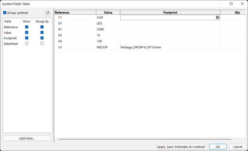
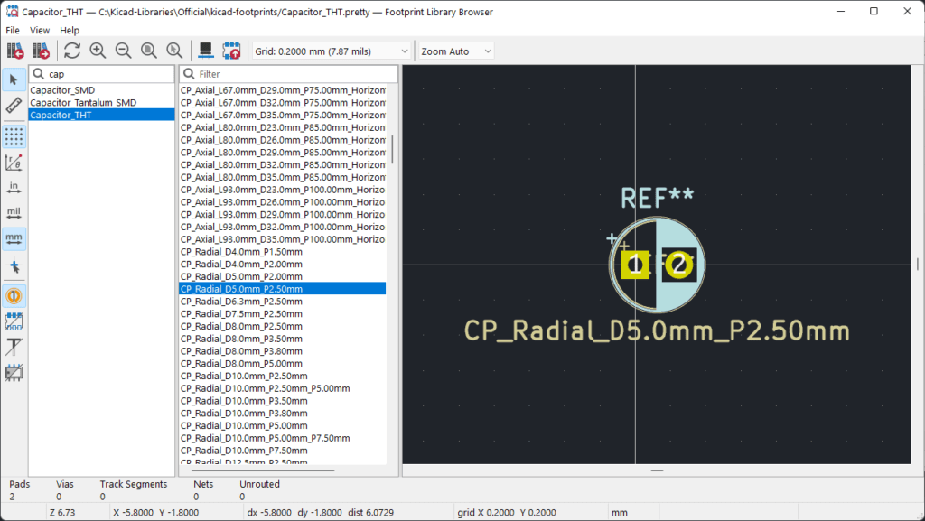
Press on the small book icon on the footprint field to open the footprint library browser. There are no filters here like we have seen on the footprint assignment tool. But we can search for keywords to easily find the library or footprint. Below you can see we have searched for a capacitor and found the through-hole (THT) capacitor footprint library. From the list, we selected the Capacitor_THT:CP_Radial_D5.0mm_P2.50mm radial capacitor footprint.
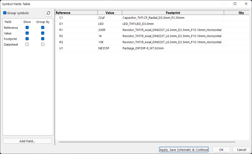
We can choose footprints for all symbols in this way. You can also copy the text field of a footprint and paste it to another symbol’s footprint field. Below you can see that we have completed assigning all the footprints.
PCB Editor
If you have followed our tutorial so far, it’s time to design the PCB now. We will use the PCB Editor of KiCad to create a PCB layout. Before that, let’s familiarize ourselves with some basics.
Grid
The PCB editor also has a grid similar to the schematic editor. You can hide the grid if you want to. The grid is more important in the PCB editor because you can customize the size, and origin and use different origins for different purposes. All elements including footprints, tracks, and text will snap to this grid (you can turn this feature off if you want, but not recommended). Therefore, the spacing between tracks and footprints will be determined by the currently selected grid size. Grid snapping makes it easy to align and arrange components on your PCB. When you want very precise control over arranging items, you can switch to a smaller grid. But for other things, such as when drawing the board outline, you can use a larger grid. We use 1.0 mm grid when drawing board outline or placing the mounting holes. It’s just easier to do in multiples of millimeters.
Origin
There are two types of origins in PCB editor.
- Sheet Origin – This is the global origin located at the top left corner of the worksheet. When you move the mouse pointer to this point, the XY coordinates will become zero.
- Drill/Place Origin – This is a user-placed origin indicated with a small red crosshair. We usually place this point at the bottom left corner of a PCB. This origin can be later used for generating Gerber files, drill and position files.
If you do not place a Drill/Place origin, everything will be still fine because the global origin will be used by default.
Layers
When working with any digital graphics on a computer, it is a good practice to slice each feature into individual layers. Designing a PCB is not different. Even though we only see a single rigid PCB once it is fabricated, the many processes carried out to make that PCB had to use different information to get the job done. The physical PCB consists of multiple layers of different materials sandwiched through different processes. Each of these material layers is represented using separate design layers. In KiCad, the layers are shown on the right side. The order of the layers is not the order of the actual stack up. All copper layers will be shown on top and then other layers.
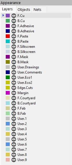
Not all layers are going to be needed for our 555-Flasher design. But let’s check what each layer is meant for. Some of the layers come in pairs and some are single.
- F.Cu & B.Cu – Front and back copper layers. This is where all the visible copper tracks will be. The tracks act as conducting paths for completing the circuit. Some people call the layers top and bottom layers. You can only draw tracks on copper layers.
- F.Adhesive & B.Adhesive – These layers are used for applying any type of adhesives. Sometimes, certain PCB parts have to be glued together, for example, rigid-flex boards. The adhesive layer shows where the adhesive should be applied. It is also can be used to apply glue before reflow soldering a PCB with components on both sides.
- F.Paste & B.Paste – Front and back paste layers. These layers contain the locations where the solder paste should be applied on the PCB. Information on this layer is not used for PCB fabrication but is used only for automatic assembly. It is also used to create a stencil.
- F.Silkscreen & B.Silkscreen – A silkscreen is the layer that contains all text labels. You will usually see them as white text on PCBs. White is not the only color for silkscreen but that’s the most commonly used one.
- F.Mask & B.Mask – Front and back mask layers. This tells where to and where to not apply the soldermask material. Soldermask is a paint-like insulating material that protects the copper layer from oxidation and prevents the overflow of solder material.
- User.Drawings – This is an auxiliary layer where you can place additional drawings which are used for documentation only and not used for PCB fabrication.
- User.Comments – This is also an auxiliary layer where you can place comments. This can be circuit explanations or specifications.
- User.Eco1 & User.Eco2 – Eco stands for Engineering Change Order. This is to include any additional information when modifying PCBs.
- Edge.Cuts – This layer contains the board outline and other cuts on the PCB. The board outline determines the physical size and shape of the PCB.
- Margin – Here you can define the margin relative to the Edge.Cuts layer.
- F.Courtyard & B.Courtyard – This contains two-dimensional bounding boxes for each component on the PCB. A bounding box is an area on the PCB where the actual component takes up space. That space can be larger than the actual footprint area. That means you can not usually place any other components inside the courtyards.
- F.Fab & B.Fab – These are fabrication layers. This is where you include all the information for the automatic assembly process. This includes polarity markers, reference designators, and component values. This layer is not needed for fabricating PCBs.
- User.1 to User.9 – These are general-purpose layers that you can use for anything.
The small colored squares adjacent to the layer names indicate the color of any graphics or text on that layer. These colors are only used for differentiating items on each layer when working with the design. They do not represent the actual PCB colors. For example, the front silkscreen layer has a light green color. But when you fabricate the PCB, you have to manually choose what color the silkscreen should be (usually white). You can change the color of the layer by double-clicking on the squares. You can also adjust the opacity or transparency. If a layer is semi-transparent, you will be able to see other layer items underneath it.
The small eye icon is a button to hide/show the layer. In addition to the layer list, you also have a list of objects and nets, and their own appearance control features. Tinker around them to see what happens when you change their appearances. There are two more features to control how the layers appear on your screen – Layer Display Options and Presets.
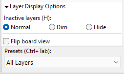
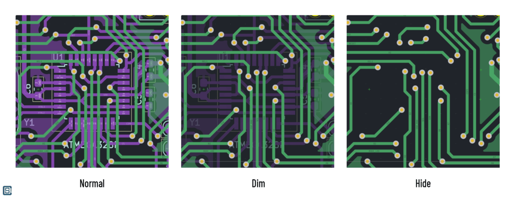
In Normal view, all of the currently enabled layers will be visible. In Dim view, all other layers except the active layer will be visible with reduced brightness. In Hide mode, only the active layer will be visible. Additionally, you can flip the board view from front to back with the checkbox option. Presets allow you to show and hide a set of layers together instead of clicking the visibility icons every time.
Footprints
Let’s talk about footprints in detail. In KiCad, footprints are created with the help of Footprint Editor. Components can have either standard packages that all manufacturers follow or non-standard ones. For example, the DIP-8 with 7.62 mm width is a standard IC package. Any IC from any manufacturer that follows the standard package dimensions will be compatible with a standard footprint. Fortunately, KiCad’s footprint library already contains thousands of such footprints. You are saved from creating everything yourself. But if the footprint for a component you want to use does not exist in the libraries, you have to either create it or you can search the internet to see if anybody else has created one. Where do we get the information to create footprints, you ask. The mechanical data of footprints will be given on the datasheet of the components.
There are generally two types of footprints; Through-Hole and Surface Mount. It is important to understand the differences between the two. Both have some advantages and disadvantages.
Through-Hole Technology (THT)
Through-hole components, as the name suggests, are inserted through holes on the PCB. THT components have leads, usually longer than needed, which you can trim after soldering. Soldering will be usually done on the opposite side of the PCB, but you can also do that on the same side. The advantages and disadvantages of using THT components are,
- They are usually large in size so that you can easily handle them.
- They are easy to assemble and disassemble on a PCB.
- Since the leads can be bent, THT components can be inserted into a non-compatible footprint, and also adjusted after soldering on the board.
- Can be used for easy prototyping with breadboards.
- The through-hole pads prevent us from placing components on the opposite side of the THT component, thus taking up more space and making the PCB larger.
- Comparatively easier to route without using many vias.
- There is a limit to how smaller they can be made.
- The excess leads become a waste and add to the cost of the product.
- Usually costlier than SMT components.
- Difficult and slow to assemble with automatic machines.
Surface Mount Technology (SMT)
Surface mount technology allows components to be placed and soldered only on either side of the PCB without wasting space on the opposite side. SMT is the newest of both. Components that use SMT are called Surface Mount Devices (SMD). So if you hear the terms SMT and SMD interchangeably, they both mean the same thing. SMT has fewer disadvantages than THT, making it the most commonly used technology for high-volume production of electronic products.
- SMT components are much smaller than their THT counterparts. Smaller components mean, they take up less space on the PCB, and thus the PCB size can be reduced. Reducing the PCB size allows an electronic product to be made smaller, saving material and production costs.
- Since SMT components are small, machines can place them on the PCBs much faster and solder them. This shortens the lead time for production.
- There is no material waste produced when using SMT components. There are no excess leads or parts to remove after soldering.
- Since SMT components have no leads but use pads, they remain firmly on the PCB if the soldering is done properly. This prevents any components from moving due to vibration or shaking.
- There are SMT components smaller than a grain of sand. They can be very difficult to handle with bare hands and therefore manually soldering small SMT components is also difficult.
- Specialized tools are needed to handle and see the SMT components on the PCB.
- There is not much space to mark the values on an SMT component. Sometimes values are completely omitted. That means, once you unpack an SMT component, it can be hard to determine the value of it, without special tools. This is especially the case with SMT capacitors.
- SMT components usually cost lesser than THT components.
- SMT components are not breadboard-friendly. They can not be used without soldering them somewhere.
- SMTs are more difficult to route.
Footprint Libraries
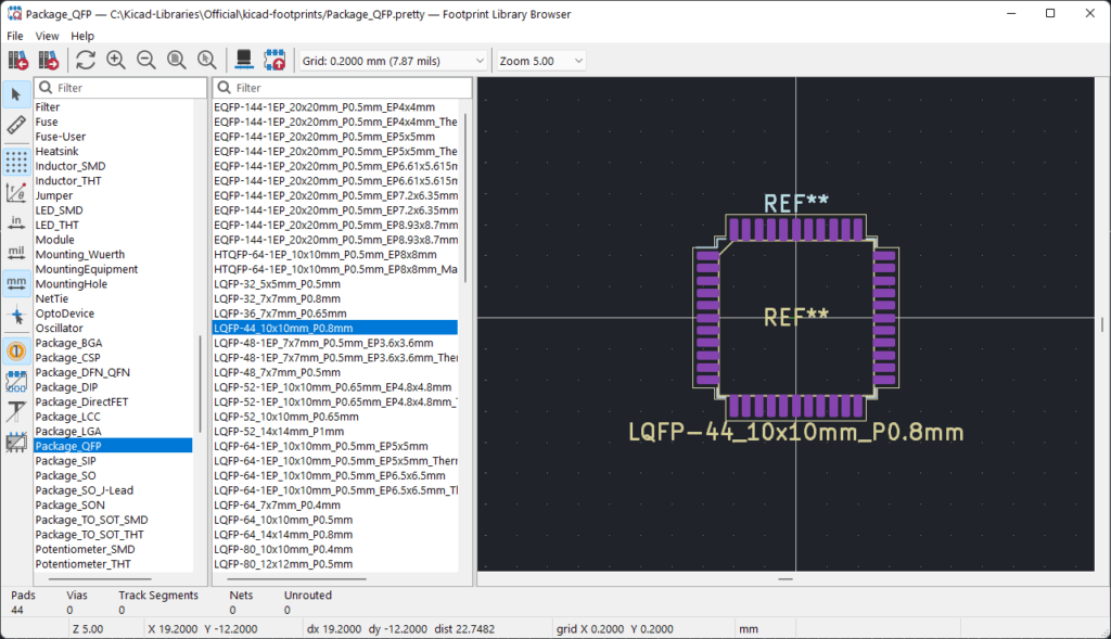
Footprints are also organized into groups called footprint libraries. A single library can contain hundreds of footprints. Each library will be a group of similar footprints. For example, all DIP packages are found in the Packages_DIP library in KiCad. All footprints must be part of any library. KiCad comes with its own standard footprint libraries with hundreds of components. You can browse all the libraries using the View → Footprint Library Browser.
Board Outline
The board outline is defined by what is on the Edge.Cuts layer. You can use any line or shape tools to draw the board outline. You can use the Line Tool, Arc Tool, or any of the shape tools. It is possible to place text or draw weird shapes on the Edge.Cuts layer but the files exported for manufacturing will be unworkable.
Make sure you set the grid size to something large, like 1 mm, so that you can easily snap the drawing tools to the grid and draw in multiples of the grid size. The most widely used shape for board outline is a rectangle or a shape using straight lines only. Such shapes are easy to draw in KiCad with the line tool. If you need a circular shape, you can use the circle tool. Other custom shapes can be drawn using a combination of all the tools. But it still can be difficult to draw complex shapes just with the tools available in KiCad. This is because KiCad is not a full-fledged mechanical CAD program. The drawing tools and constraints available are limited. In such a case, you have to use any other mechanical CAD software to create the board outline. The drawing should consist of only lines with no intersecting lines and the shape must be completely enclosed. For example, we use Autodesk Fusion 360 for creating custom board outlines. Then we export the drawing to DXF format. DXF is a vector format and it is supported by KiCad and you can import the DXF file using KiCad’s import graphics menu at File → Import → Graphics. You can use this feature to import DXF or SVG graphics to any layer. You just need to select the destination layer correctly.
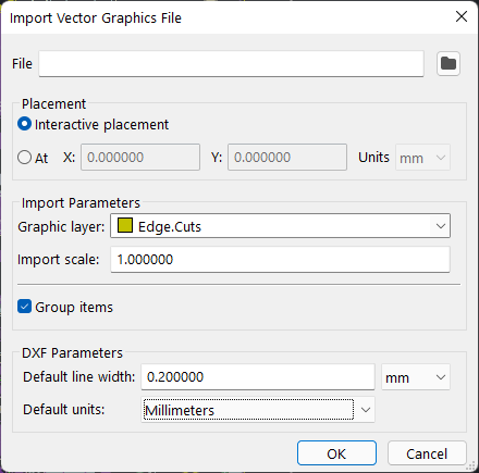
Choose the file from your computer using the small folder icon. You can place the graphics anywhere on the sheet using interactive placement. If you know the specific position, you can enter the coordinates. If you are importing a board outline, choose Edge.Cuts as destination layer. Import scale is to make your graphics larger or smaller relative to their original size. To make the process smooth, always prepare graphics in 1:1 scale and import with scale 1.0. Grouping the imported graphics can make it easy to select and move the graphics once it is placed.
If you are importing a DXF file, the line thickness for importing can be specified. This thickness is only a visual representation of the board outline. The line thickness has nothing to do with the actual board shape or size. Only the line coordinates will be used for the PCB routing process.
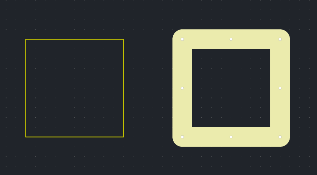
See the above two rectangles with the same 10 x 10 mm size. These squares are on the Edge.Cuts layer. The first square has a line thickness of 0.1 mm and the second has 2 mm line thickness. When you fabricate these PCBs, both will come with the same 10 x 10 mm size. That means, the line thickness never matters for Edge.Cuts layer. The best size for line thickness for board outline is 0.1mm. You can use this size when importing the board outline as DXF. Also, choose the unit to whatever unit with which you have drawn the graphics. If you used inches for drawing the graphics on a CAD program, you must also select inches while importing. Otherwise, your design will look smaller or larger than the actual size.
Tracks
Tracks, sometimes called traces, are the physical equivalent of wires on a schematic. They electrically connect components soldered on a PCB. Tracks can be drawn only on the copper layers and they connect footprints to complete an electrical circuit. Tracks can have different sizes, shapes, and other properties. The process of drawing tracks is called routing. The minimum width of the tracks and spacing between any other items will be specified by the manufacturer. You have to follow these specifications when designing your PCBs. If the specs are not correct, the manufacturer may reject your design.
In KiCad, track widths can be specified by going to File → Board Setup → Pre-defined Sizes. When you first open a design, the lists will be empty. You can simply type in a new value or delete existing ones. The default unit will be mm, but you can also explicitly specify the unit as 0.4 mm, 10 mil, etc. These sizes will be available as a drop-down list when you are designing the PCB. The size currently selected from the list will be used when you use the routing tool.
Track sizes can be any arbitrary value. Any size can be printed. But their size also determines the max current they can carry safely, and a few other parameters. This calculation has to also consider the thickness of the copper layers. For example, 35 micron (1/1000,000 of a meter) or 1 oz is probably the most used copper thickness. There are smaller and larger thicknesses than 35 um. Track properties also determine their impedance (resistance to varying signals), maximum signal frequency, and EMI generation. For basic designs, you don’t have to worry about such things.
Plated and Non-Plated Holes
Holes on a PCB can serve many purposes, and depending on their purposes they can have different properties. Holes are first created by drilling; either using drill bits or laser beams. These holes are then processed in various ways to give them the required properties. Two terms you will commonly hear about holes are Plated Through Holes (PTH) and Non-Plated Through Holes (NPTH). As you can see in the illustration below, holes can be actually deposited with copper or other materials to make them conductive, just like a copper track. Such holes can connect multiple copper layers on a PCB. For example, on a two-layer PCB, a PTH can connect a track on the front side to the track on the opposite side. This is why routing circuits on a two-layer board is easier than on a single-layer PCB, in which you will need to use jumpers more often.
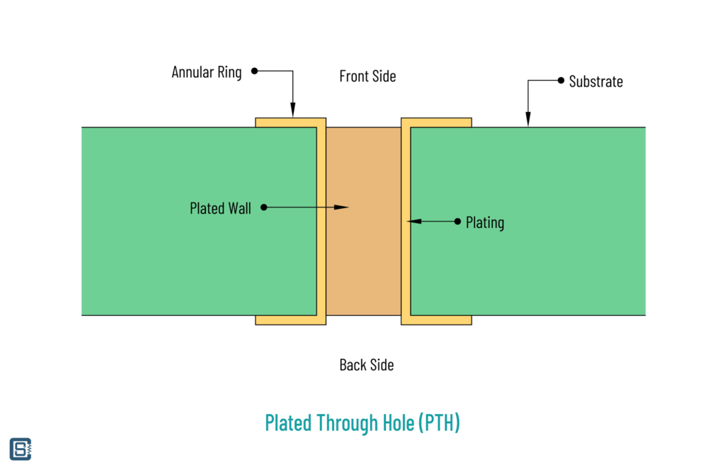
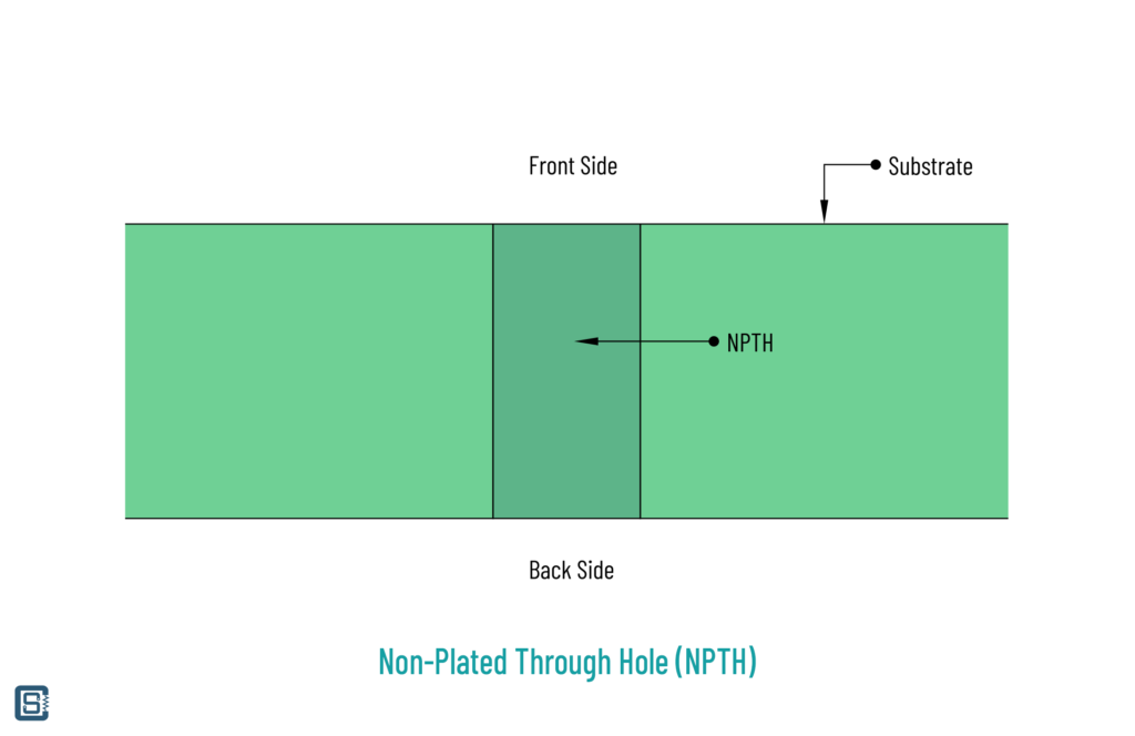
A Non-Plated hole has no conductive path on its wall. NPTH is a bare mechanical hole that is mainly used as a mounting hole or internal cuts. You can create both PTH and NPTH holes in KiCad. The “Through” in the terms means the holes make their way completely from one side to the other. If you are wondering why we had to be specific about such a term is because we can indeed have holes that start at one side but do not come out through the other side. More about them in the next section.
Vias
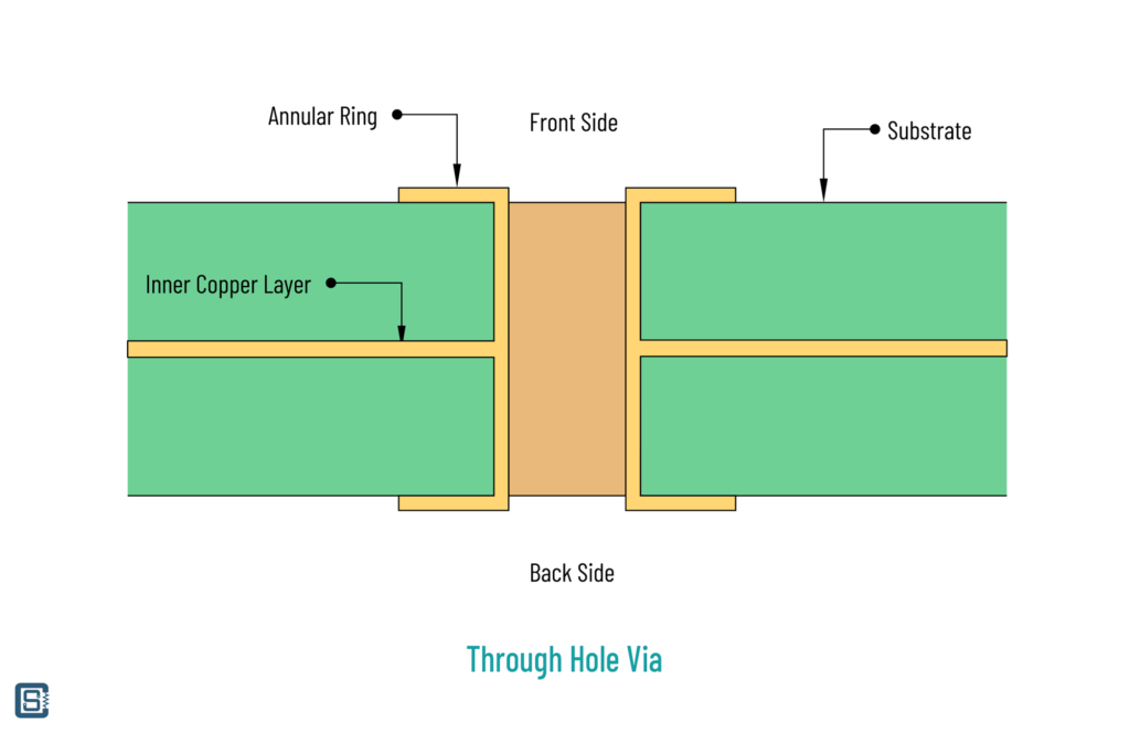
Vias are also plated through-holes but they only serve as interconnections between different conducting layers of a PCB. Vias will be automatically placed when you route a track. In KiCad, you can press V when the routing tool is active, to place a via. The size of the via will be smaller than a PTH intended for a through-hole component. Vias have two size parameters; their diameter and drill size. The coper ring that is left after the drilling process is called Annular Ring. PCB manufacturers will specify the minimum annular ring size you can have. You must make sure the sizes are within the limits.
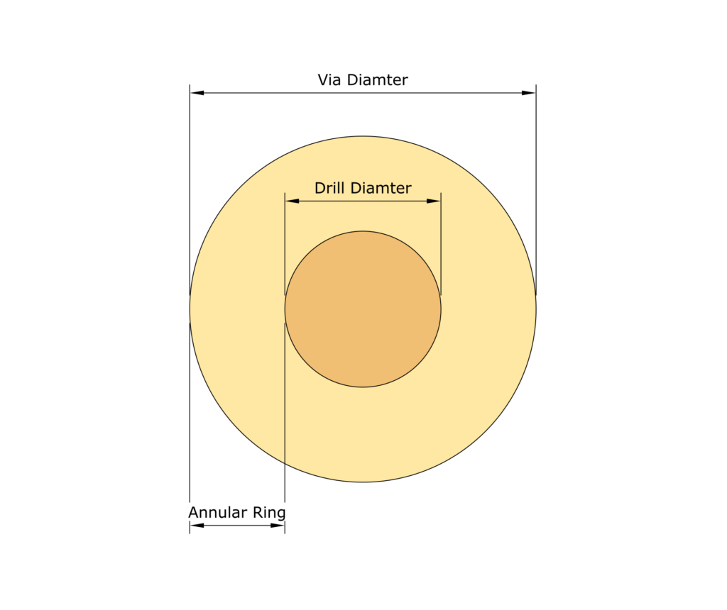
In KiCad, you can save a set of predefined via sizes by entering diameter and drill size. For example, a commonly used size is 0.8 mm diameter and 0.4 mm drill. This leaves 0.2 mm annular ring. If the annular ring is too small, it can cause faulty PCBs, due to drill shifting, that will fail electrical testing during production or at a later stage when the device is deployed. A complementary design choice to prevent annular ring issues is to add teardrops, a kind of filleting to tracks and vias. This adds extra copper to the vias without affecting the overall design. KiCad does not natively support teardrops as of now, but you can use this Teardrops plugin instead.
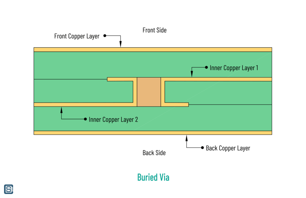
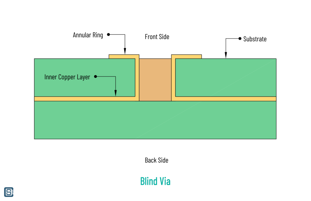
And that’s not all about vias. The type of via we just explained is a Through-Hole Via, which means one that has drilled hole entering from one side and exiting through the opposite side. It may connect two or more copper layers. But there are vias that do not pass through the complete material. Instead, they stop at some intermediate layer. Such vias are applicable to multi-layer PCBs (more than two layers) only. Such vias are called Blind Vias. Another type of via is called a Buried Via, which connects two or more inner layers. This means, buried vias will not be visible from either the front or backside, once the PCB is fabricated. Only by making a sectional cut, you can see them. KiCad supports all types of vias.
Ratsnest
This has nothing to do with rats, but it’s better to have names for everything. When you import a schematic (fully annotated and footprint assigned) to the PCB editor, all the footprints will be grouped together and their interconnections will be displayed as lines called airwires, starting and ending at footprint pads. Ratsnest is the visual equivalent of a netlist.
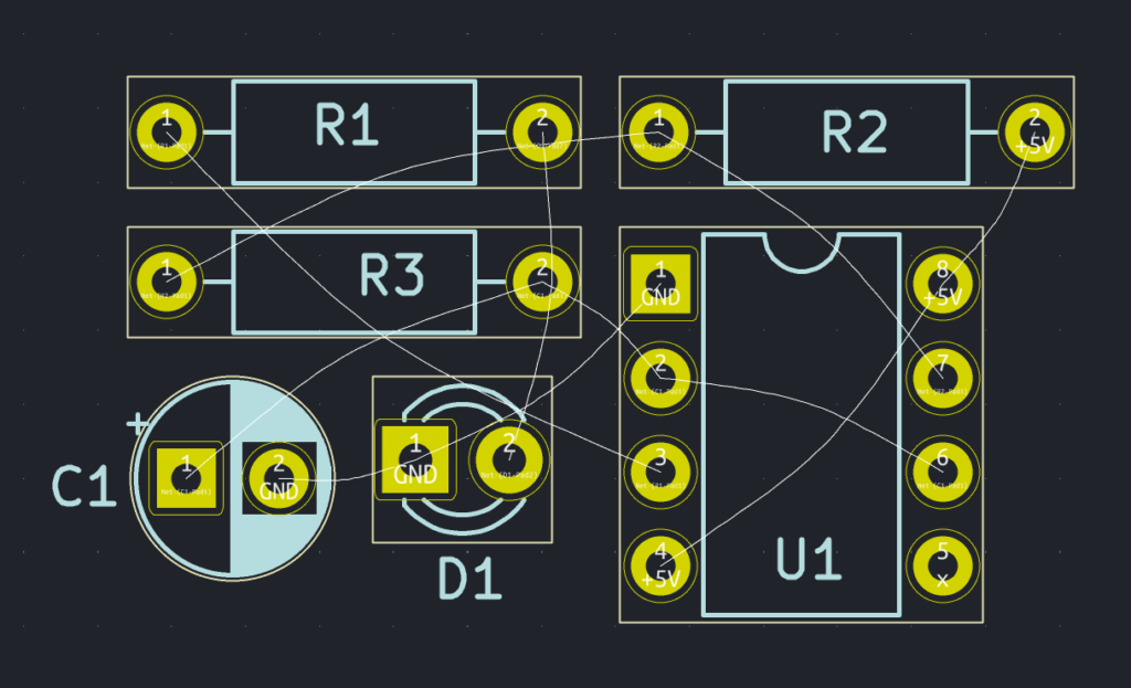
To import the schematic to PCB, first, open the PCB editor and go to Tools → Update PCB from Schematic. This will open a window as shown below.
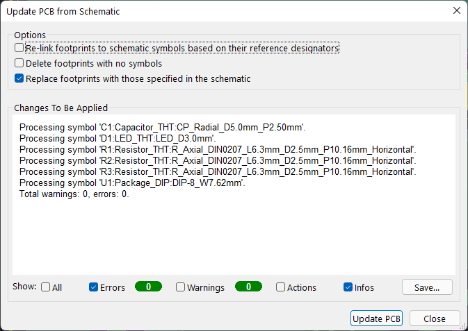
You have three options,
- Re-link footprints to schematic symbols based on their reference designators – KiCad uses unique GUID/UUIDs (Globally/Universally Unique ID) to internally naming footprints and schematic symbols. For example, you may have a symbol called
R1on your schematic. This symbol will be also assigned with a GUID by the software, and we can’t know what it is (unless you open the schematic file on a text editor). When you import this schematic to a new PCB, the footprint and schematic symbol will be linked together by default. Now suppose that you have changed the symbol reference fromR1toR3and imported the change to the PCB. Since symbols and footprints are linked through GUIDs, the now changedR3will be the symbol that represents the same old footprint on the PCB. This might not seem like an issue when you only have one component. But this can become problematic when you have more components and you swap many of the reference designators (for example when you do geometric annotation). The first option on the new dialog resets the GUID-based relation and explicitly uses reference designators as linkages. - Delete footprints with no symbols – this will do what it says. If you have a footprint of any kind that is not linked to a schematic symbol on your schematic, it will be deleted to keep parity between schematic and PCB. For example, you may add mounting holes, special symbols, etc. on your PCB from the PCB editor itself. When you do this, there will be nothing linking those new footprints to the schematic. So if you update your PCB with this option on, all of them will be deleted. So be careful when you enable this option.
- Replace footprints with those specified in the schematic – this is the most used option. It allows you to import the complete list of footprints even to a new PCB. In case you changed a footprint assignment later, on an already imported schematic, the existing footprints will be replaced with the new ones. But you must also remember that you are able to change a footprint within the PCB editor. When you have made such [unsynced] changes, whatever changes you have made will be lost after performing an import. So make sure you either sync PCB changes back to schematic, or disable this option when importing.
For importing our 555-Flasher schematic for the first time, we only need the third option and then press Update PCB button. You can now see the footprints and ratsnest connecting them. The ratsnest can be disabled from the left pane, if needed.
Selection Filter
The PCB file is just a graphic file containing multiple layers stacked on one another, and each layer can have hundreds or thousands of items on it. Our view of the PCB is limited by just a two-dimensional screen. When you show all the layers together, it will appear as a spaghetti mess. Showing and hiding individual layers is one way to focus on a few layers at a time. But what if you want to select specific items from the layers by either clicking or marquee selection? For example, you could change the size of vias if you select them together and change properties. But Shift + left clicking on each via is not practical. The Selection Filter allows you to restrict your selections to specific items on the PCB.
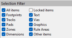
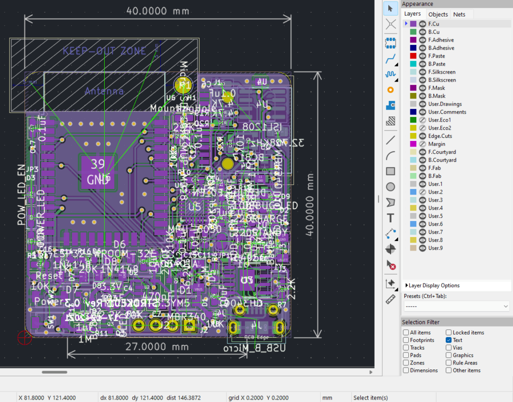
The type of items you can select is limited by what is supported by the filter, but you have most of the options you’ll ever need. Use the checkboxes to enable or disable the filters. For example, enabling only the Text filter will allow you to select silkscreen items and other text by clicking or marquee selection. No other items will be selected even if you click right on them.
Manual Routing
Routing is the process of drawing tracks on the copper layers. There are two methods to perform routing; either Automatic or Manual. In automatic routing, EDA software uses one or more algorithms to find an optimized layout for routing all the tracks. The autorouter may use vias or jumpers during the process. Sometimes this yields a 100% result, where all the tracks will be routed. Other times, a few are left for you to manually route.
Autorouter is a quick way of routing prototype PCBs where track lengths, positions, stacking, etc. don’t matter much. But when you are working with a crucial design and you need maximum control over the process, you have to do manual routing. KiCad V6 only supports manual routing. There is a way to autoroute KiCad PCB files, but we won’t cover that here for now.
Let’s route our 555-Flasher PCB. We have already imported the footprints to the PCB editor, but we haven’t added the board outline yet. To add a board outline,
- Select the Edge.Cuts layer.
- Set the grid to 1.0 mm.
- Use the rectangle tool to draw a rectangle around all the footprints.
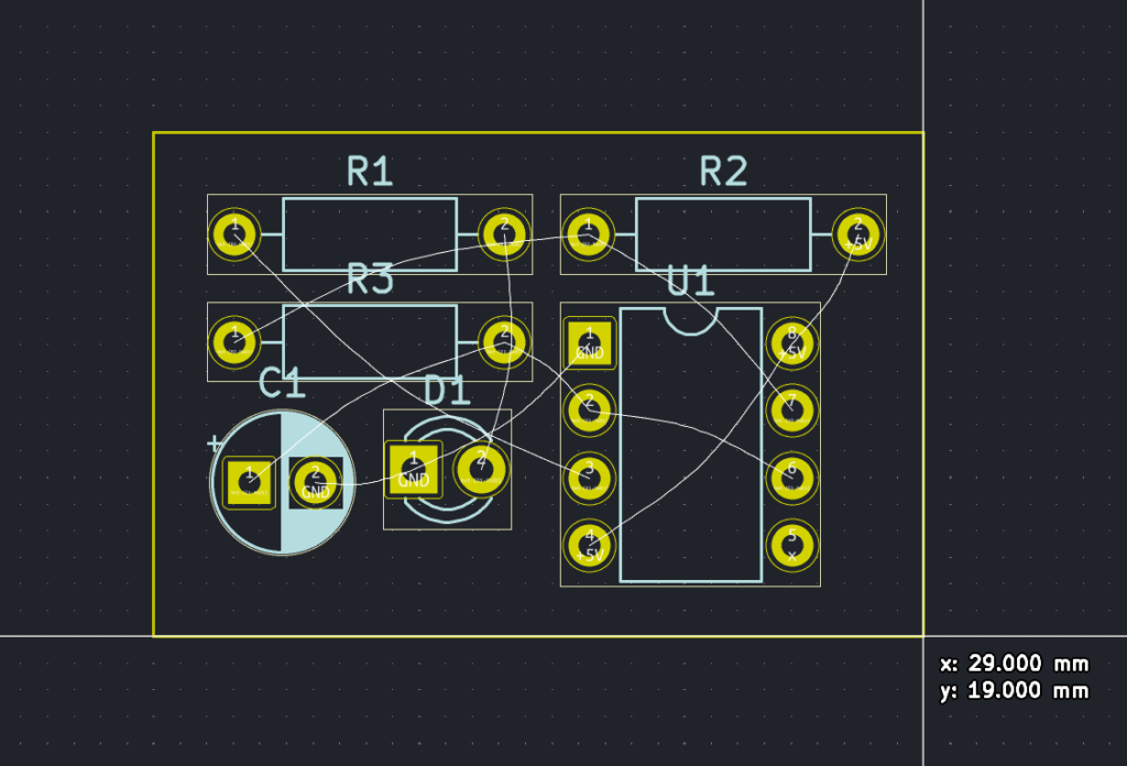
Now change the grid size to something like 0.2 mm and choose the routing tool. We will route on the backside first, so choose B.Cu layer. There won’t be any predefined sizes for track or vias yet. So add a few sizes such as 0.4, 0.6, 0.8, and 1 mm to the track sizes. The default via size is 0.4/0.8 mm which is sufficient.
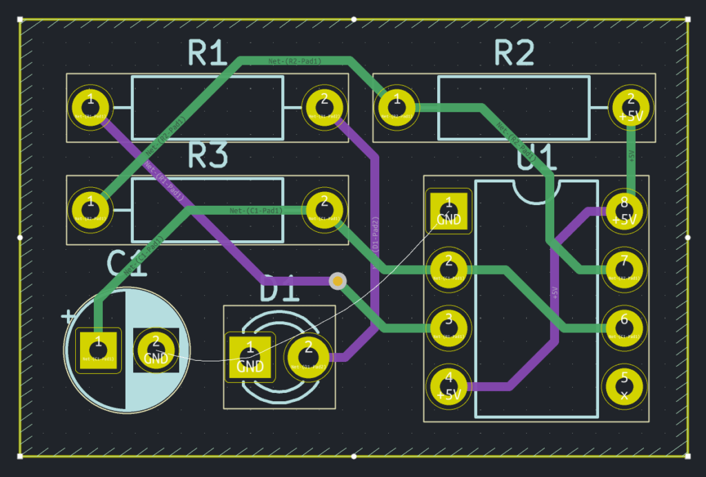
Now choose 0.4 mm as the track size and start routing. When you click on any pads, the tracks and all pads that should be connected to them will be highlighted. This helps you decide which direction you should move the track. Usually, we connect the track to the nearest footprint. When you finish the process, a complete track will be laid out. The ratsnest line for those two pads will also disappear, indicating that the pads are now connected by copper. You can cancel the operation by pressing Esc.
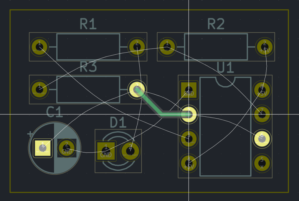
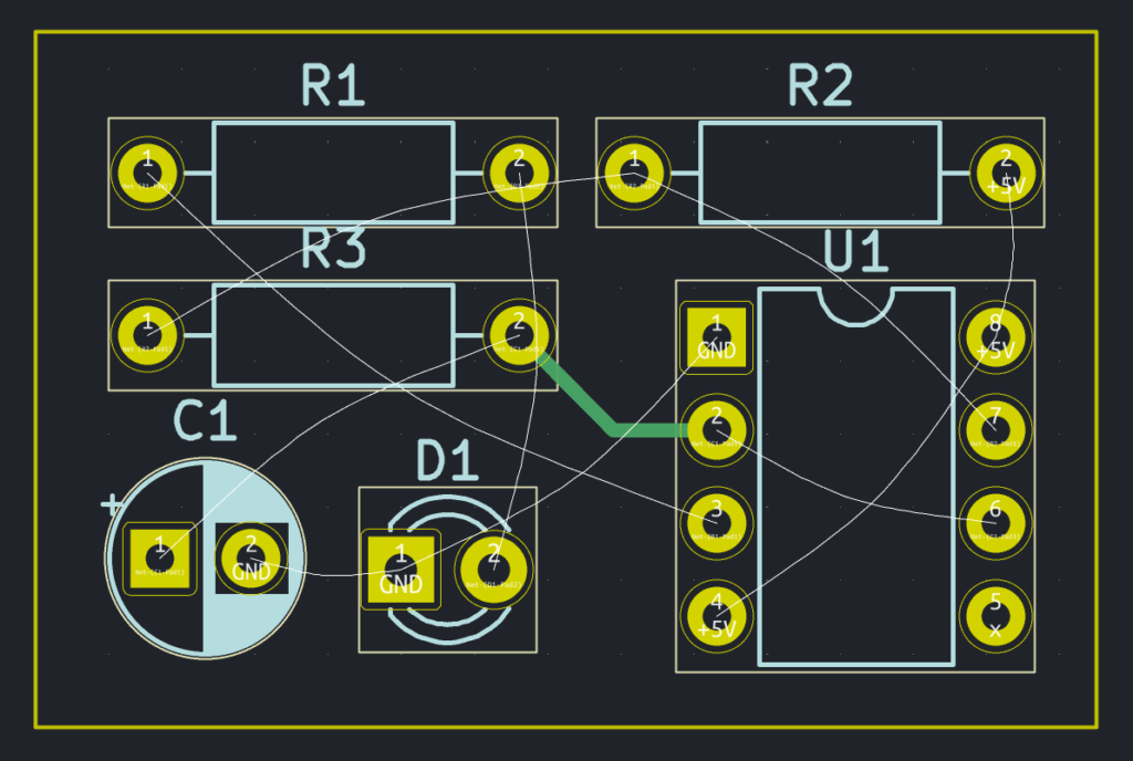
Now continue routing the rest of the nets, by connecting the nearest pads. Do not route GND nets yet. We will do that at the end with filled zones. We have routed a few tracks as shown below and how you have routed may be different and that’s okay. Observe the following scenario now. We want to route pin 2 of R2 and pin 2 of D1. But since we already have a track crossing the path, we can not simply draw a new track over it. If you draw intersecting tracks on the same layer, it will short the circuits. KiCad prevents this from not allowing you to draw intersecting tracks of different nets. There are three ways to accomplish the task in this case.
1. Route through a different area by walking around other footprints or tracks, avoiding any intersections.
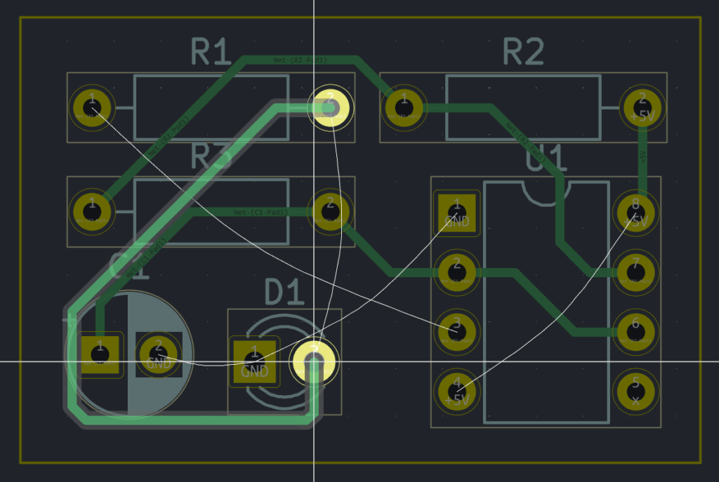
Most times, this method creates long and ugly-looking tracks that are hard to manage. Such tracks can also complicate the routing and debugging later. So the rule of thumb is to keep your tracks as short and neat as possible without too many bends or direction changes.
2. Use vias to jump across one or more tracks on the way.
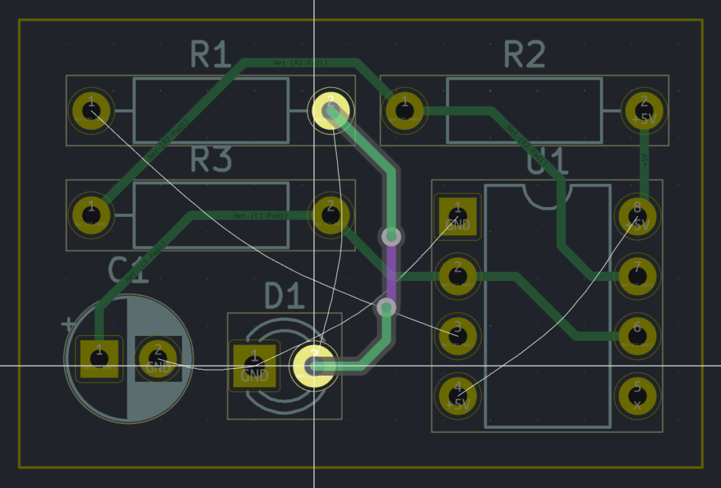
We have used two vias just to keep the ending part of the track on the same back layer. This could be accomplished with just one via otherwise. You can press V to place a through-hole via when the routing tool is active. For double layer PCBs, whenever you place a new via, the routing layer changes to the next copper layer. If you want to explicitly change the layer, press F key to switch between copper layers. Using vias is only possible on PCBs with more than one layer. Since the vias can connect tracks from the front side to the backside, they help us to jump over obstacles and keep tracks short and neat.
3. Route on a different copper layer.
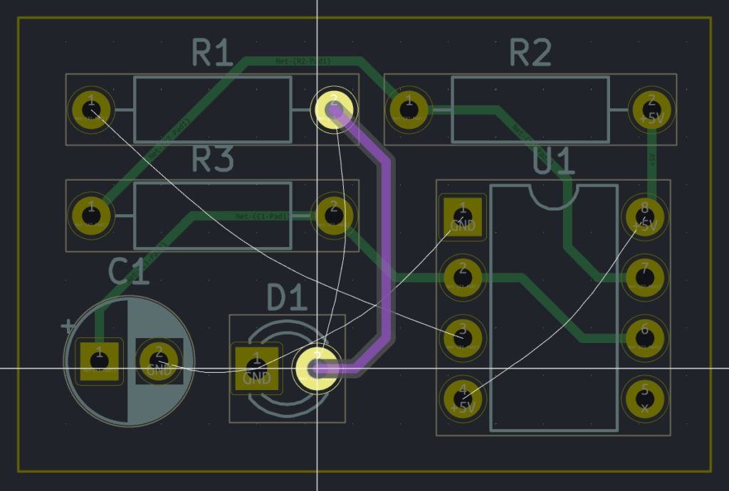
This is straightforward. Just use a different copper layer to route the new track. This keeps the track short and neat but without using any vias. Tracks that are completely on one side are easier to debug when you get the PCB.
Finally, we have routed all the tracks except the GND net. We will use filled copper zones to connect all our GND pads. This is explained in the next section.
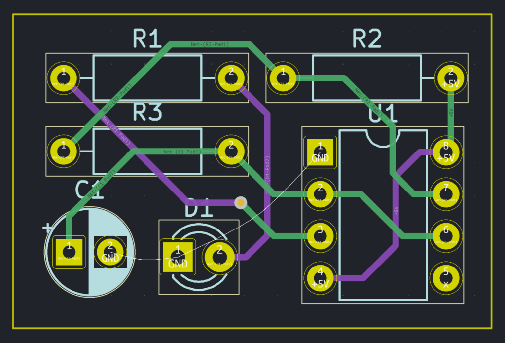
Filled Zones
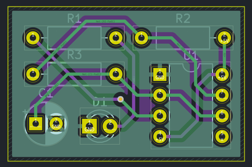
Filled zones are large areas of copper that are laid out automatically. They are usually used for creating GND planes. The GND or -VE line of power supplies and batteries are used as a common reference in most systems. All other voltages are measured with respect to this line. Therefore it is important that all parts of our circuit and PCB see the same potential on the GND line. If it is not the same, tiny voltage differences will cause ground loops and interfere with the system’s performance. External noise can also induce EMF on copper tracks and thus changing potentials at various points. Also, GND is a line that sinks currents from all other points. So this track must be the thickest of all tracks with the lowest resistance.
A ground plane acts as a low resistance/impedance path for sinking all currents and maintaining uniform reference potential at all points on the PCB. It also shields signals from external noise by accepting them as common-mode noise. Ground planes also reduce copper wastage and make your PCBs aesthetically pleasing.
Filled zones are used for other signals as well. To create a filled zone, first, change the grid size to 1 mm. This is so that we can draw the zone easily. Then choose the Add a filled zone tool. Click on the top-left point of the PCB outline. You will see a new window the moment you click.
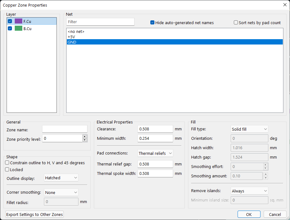
This window lets you set all properties of the zone before placing it. The most important property is the net used for the zone. Since we only have GND pins left to connect, we will make the zone a ground plane. Choose GND from the netlist. Now you can specify on which layers the zone should be filled. We will set this to both Front and Back by selecting the layers on the layers list. There are many other properties whose values are filled by default. For example, clearance is the space between the edge of the copper zone and any other copper items such as tracks. You can always change these properties after placing the zone and refilling it. So leave other settings as-is for now. You have to finish drawing the copper zone once the settings are set.
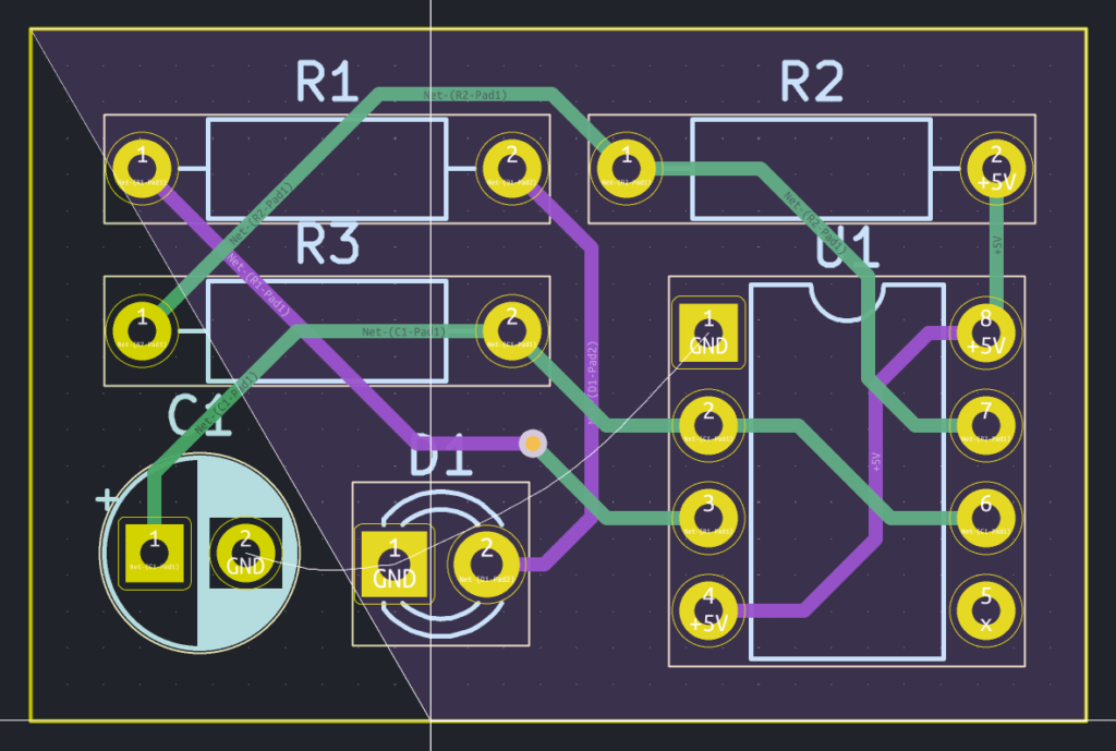
Once you finish drawing the zone, a hatched outline will show up. The zone is not filled yet but only placed.
To fill the zone, go to Edit → Fill All Zones or simply press B key. Filling the zone will also connect all the GND pins and thus finishing the routing. We have completely routed our first PCB 🥳 Every time you make changes to the tracks or move a footprint, you need to refill the zones manually. If the zones are not refilled it can spoil your designs. So always press B after making changes.
Now you may rearrange the silkscreen labels using the move tool.
Keepout Area
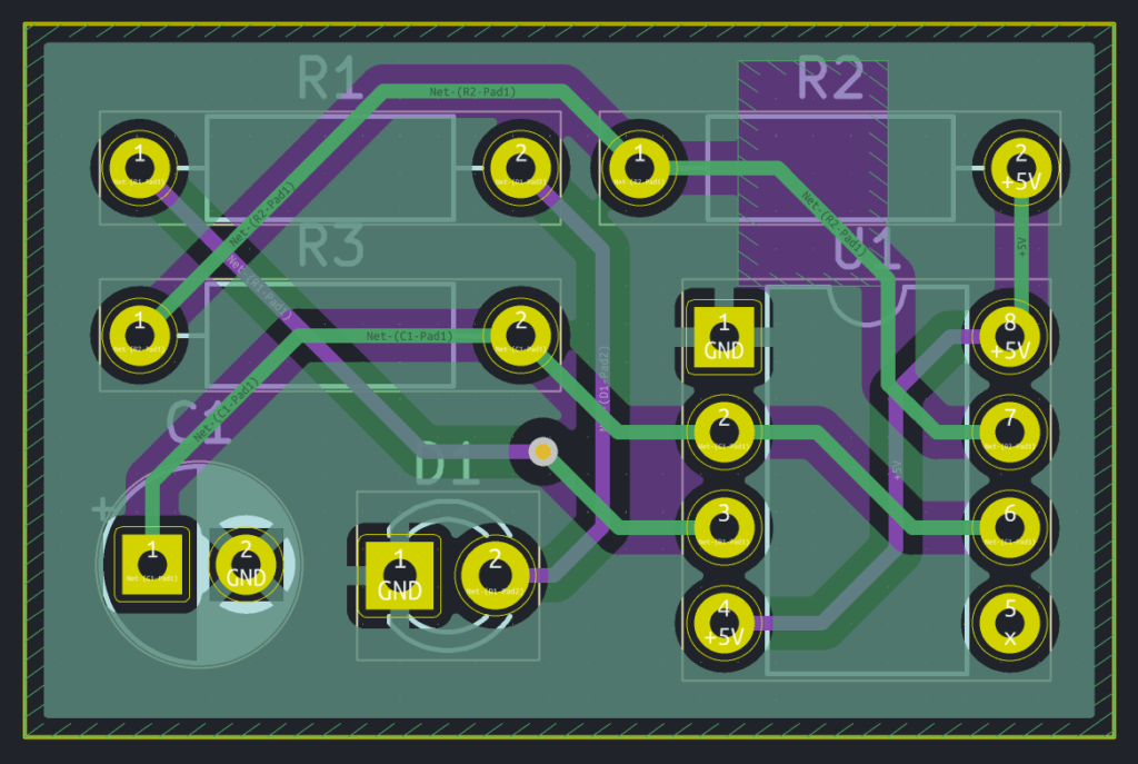
Sometimes you want to exclude certain areas of your PCB from having copper fills, tracks, or vias. Such zones are called keepout zones. Keepout zones can be specified just like we do with filled zones. Use the Add a rule area tool to draw a keepout zone. We will simply draw a rectangle at a random place to show how keeptout areas work.
You get a new window as soon as you click anywhere on the window. You can specify which layers the rule area must apply, and which items to be kept out from the area.
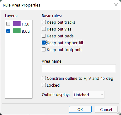
We will just exclude the copper fill from the rule area and apply it only on the back layer. Press OK to finish the setting and complete the drawing of the area. Once you draw the rule area, you have to refill the zones for the change to take place.
Design Rules Checker (DRC)
Same as we have Electrical Rules Checker (ERC) on the schematic editor, we also have Design Rules Checker (DRC) for PCBs. This is an automated testing of the design and reporting of possible errors. No design is perfect, and as humans, we make a lot of mistakes. The software can tell us about potential problems. That’s why it is important to run DRC once you finished your design. We must specify the rules before we can use DRC. These rules can also be customized.
To run DRC, got to Inspect → Design Rules Checker on PCB editor. This will open a new window with a few options and a message area. Keep the options as they are, and run the DRC once. If your design did not have any issues, you will see zero errors.
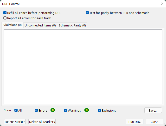
Since our 555-Flasher PCB did not have any issues, let’s add one, shall we? We will short two nets by manually placing a copper track on the pads. KiCad won’t allow you to place this with the interactive routing tool, but you can use the move tool to move a copper track anywhere on the design. We have shorted the pads of R1 and R3 as shown below.
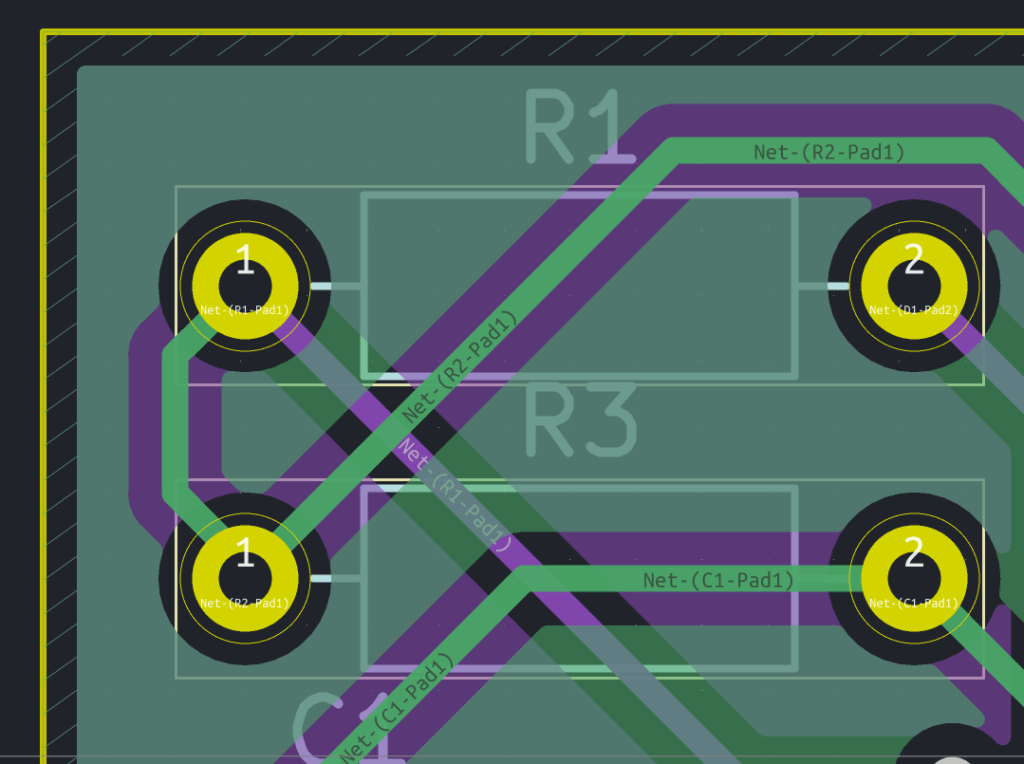
Now if we run the DRC again, you will see the error show up as a clearance violation. It will also add a marker on the design where the error is and it will be highlighted when we click the error on the list.
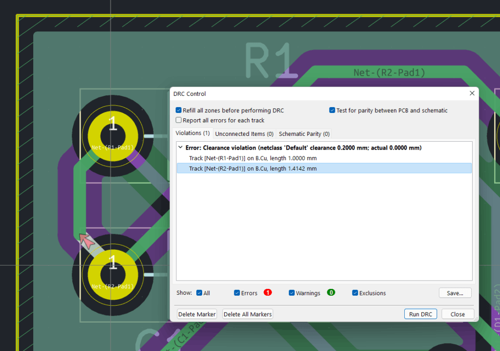
The markers will remain there until we fix the issues and run the DRC again. You can manually delete all the markers by pressing Delete All Makers. Another way is to suppress the error manually, by right-clicking on the error on the list and choosing to exclude it. But be really careful when doing this. If you exclude a violation without thinking of the side effects, the software will no longer warn you even if you were going to run off a cliff.
Warnings are less severe than errors. They just tell you about possible improvements in the design. The severity of each type of violation can be configured from File → Board Setup → Design Rules → Violation Severity.
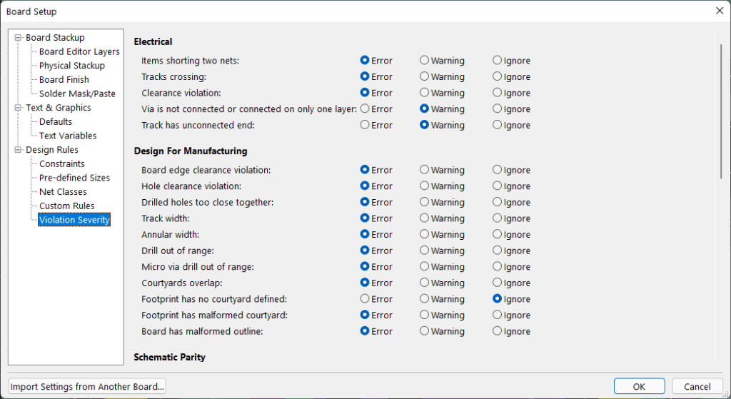
Updating PCB from Schematic
Changes you make from the PCB editor can be exported to the schematic editor by going to Tools → Update Schematic from PCB. For example, you may change the footprint assignment of a component or change its value. Such changes can be synced back to the schematic to maintain parity. If you don’t export the changes made on the PCB, all changes will be lost when you import any changes from the schematic to PCB later.
3D Shapes
KiCad has a 3D viewer of its own. In order to show your PCB in a 3D viewer, all components must have a 3D shape associated with them. If a 3D shape is not available, you will see blank space. Fortunately, KiCad’s standard libraries contain hundreds if not thousands of 3D shapes. These default associations will be imported automatically when you add a component. Note that the 3D shapes are associated with footprints only, not schematic symbols.
To see the 3D shape of a footprint, open the properties and open the 3D Models tab. This window will show the path of the current 3D shape and other settings for orientation and positioning. WRL is the format that is displayed by default. But KiCad also can show STP/STEP format models. STEP models are mainly used when you export the 3D model of your board. If you have a footprint with a missing 3D model, you could try searching on the internet to see if anyone has published a STEP model of it. If you find one, you can download and add it to the 3D models path on the properties of the footprint. If you couldn’t find one, you will need to design one yourself. But make sure you share the model you created with the world so that someone searching for it somewhere else in the world can find it. You may also submit the new 3D models to KiCad’s official repository.
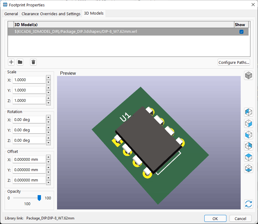
3D Viewer
Got to View → 3D Viewer or press Alt + 3 to open the 3D viewer. You can use the mouse to pan, zoom, and orbit around the board. You can also selectively hide/show items on the board. If you go to PCB editor and select a footprint, and then open the 3D viewer, the part you selected will be highlighted in green on the 3D viewer.
The 3D viewer is an amazing tool to verify the physical/mechanical aspects of your PCB designs before it gets manufactured. You can even view a more realistic raytraced render of your PCB. You have two types of 3D projections available; Orthographic and Perspective. The orthographic projection will show a dimensionally accurate view, where all lines of the same length will be rendered equal. The perspective view shows how we actually see things in real life. Large distant objects will appear small and small closer objects will appear large, regardless of their sizes. Play around with the options to see what you can do with the 3D viewer.
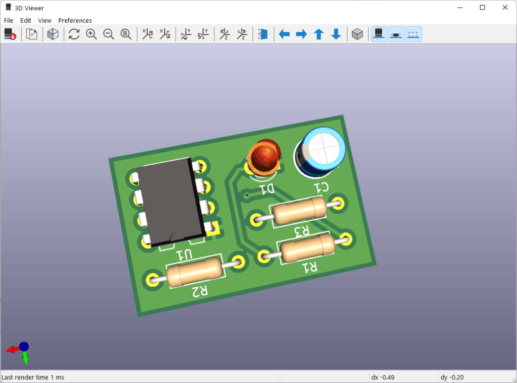
Gerbers
Gerber is the file format used to send PCB design files to a fabrication house. Gerber is a standard vector manufacturing file format supported by all fabrication houses and you can export them from KiCad under File → Fabrication Outputs → Gerbers. We have a complete tutorial on exporting Gerbers in a previous post.
Bill of Materials
Bills of Materials (BoM) is a list of all components on your PCB. The list will include the reference designators, values, quantities, footprints, and other details. The BoM is required for sending to a component distributor so that you can buy the parts. You also need to send this to the PCB assembly service provider to do automatic assembly of your PCBs. We have covered all details of PCB assembly and the files you need to generate for PCB assembly, in a previous post. You can export the BoM from the PCB editor by going to File → Fabrication Outputs → BoM.
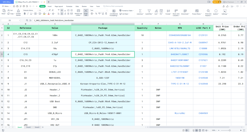
Position Files
Position file or centroid file is also related to the automatic assembly of a PCB. This file tells a Pick and Place machine (PnP) where to place each component in what orientation. Position files can be generated from File → Fabrication Outputs → Component Placement. We also have covered this in detail in our previously mentioned post.
Versioning
Versioning is the process of creating snapshots of your designs as you make new changes. Version or revision numbers are usually placed somewhere on the PCB to indicate which design it is. Issues with one version may be fixed on the next version. So it is important to keep track of important versions and have a reference for the future. KiCad unfortunately does not directly support any version control. But since KiCad files are text-based, we can still use any other version control software such as Git.
You can also save entire projects using Save As option and name the project file with a revision number. Make sure you add design details and versions on the worksheets also. We also export complementary files whenever we create a new version.
That’s the end of this tutorial. We would love your feedback on this. Please let us know if we missed any important aspects or made a mistake on the way.
Happy KiCading 😉
Links
- Getting Started with KiCad – official documentation
- Creating Circuit Boards with KiCad 6 – a great video tutorial from shabaz
- Donate to KiCad
- Download KiCad 6
- Interactive HTML BoM – Plugin
- Board2PDF – Plugin
- KiBuzzard – Plugin
- KiKit – Plugin
- PCB Action Tools – Plugin
- Teardrops – Plugin
Short Link
- Short URL to this page – https://circuitstate.com/learnki6


