MITAYI Pico RP2040 r0.5 – Open-Source Microcontroller Development Board – Schematic, PCB and Assembly
The complete documentation for design revision 0.5 of the MITAYI Pico RP2040 open-source microcontroller development board from CIRCUITSTATE. Read about the schematic design, PCB design and assembly.
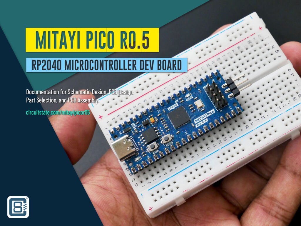
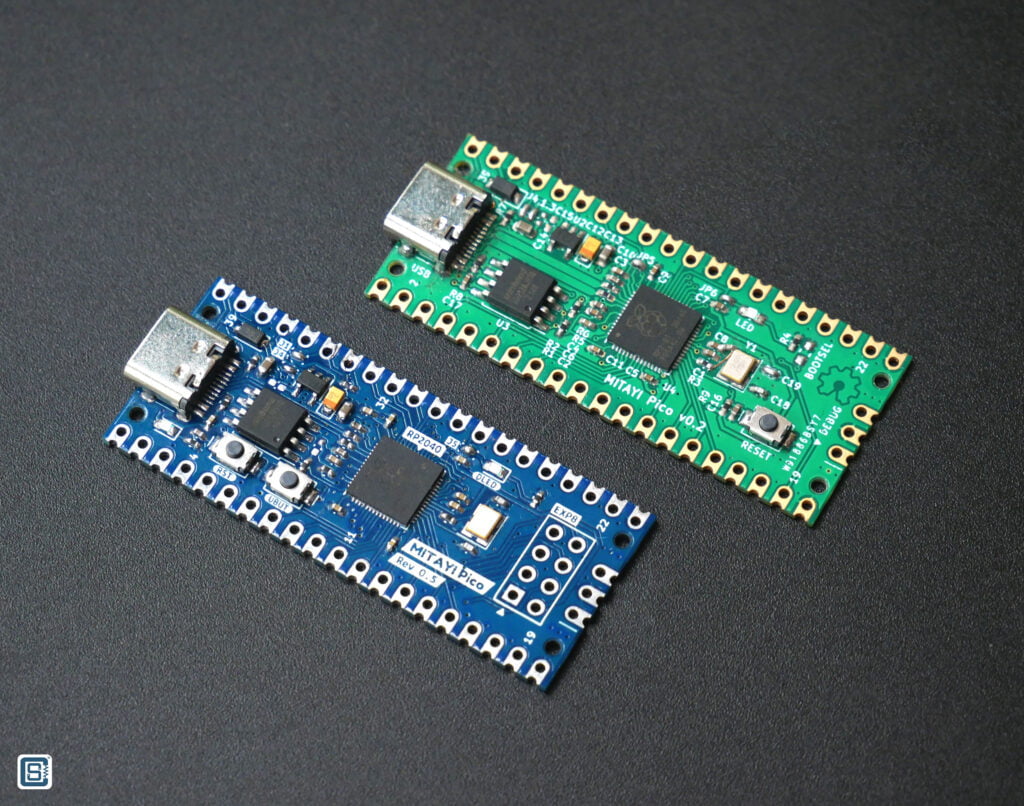
MITAYI is a series of RP2040-based microcontroller development boards from CIRCUITSTATE Electronics. MITAYI Pico is the first one in this series and we have the second release version r0.5 out now. In this post, we will discuss about all the changes and updates we have incorporated since the release of the r0.2 design which we assembled and tested. MITAYI is a completely open-source hardware released under an MIT license and so you can download the original source files and use them for any purpose. The version r0.5 is close to the production variant we have in mind. When it is finally ready, we will release it as the r1.0 and you will be able to them.
Features & Specifications
Some of the features remain unchanged while some others have changed between r0.2 and r0.5. To make this post standalone and complete, we will relist all the features and specs again, while changes will be specifically mentioned.
RP2040
- Dual ARM Cortex-M0+ @ 133MHz
- On-chip PLL allows variable core frequency
- 264kByte high-performance SRAM in six independent banks
- Support for up to 16MB of off-chip Flash memory via dedicated QSPI bus with eXecute In Place (XIP)
- DMA controller
- Fully-connected AHB crossbar
- Interpolator and integer divider peripherals
- On-chip programmable LDO to generate the core voltage
- 2 × on-chip PLLs to generate USB and core clocks
- 30 multi-function General Purpose IO (4 can be used for ADC)
- 1.8-3.3V IO Voltage (NOTE: Pico IO voltage is fixed at 3.3V)
- 12-bit 500ksps Analog to Digital Converter (ADC)
- Peripherals
- 2 × UART
- 2 × SPI controller
- 2 × I2C controller
- 16 × PWM channel
- USB 1.1 controller and PHY, with host and device support
- 8 × PIO state machine
- 2 × Programmable IO (PIO) blocks, 8 state machines total
- Flexible, user-programmable high-speed IO
- Can emulate interfaces such as SD Card and VGA
- QFN-56 7x7mm package
Mitayi Pico RP2040 r0.5
Features that remain unchanged are shown in green and changes and new features are shown in blue.
| RP2040 dual-core, 133MHz ARM Cortex M0+ microcontroller. |
| 16 MB Flash memory in SOIC-8 package. |
| Power and Debug LED indicators. |
We retain the dual USB (USB-C and USB-Micro) footprints on the PCB. But USB-Micro pads are no longer exposed to prevent a USB-C connector from shorting the pads. |
We no longer have dual voltage regulators. The AMS1117 footprint has been removed and now we only have the MIC5219-3.3. |
| Reset button. |
| New BOOTSEL button named UBUT. This button can function as BOOTSEL button or as a generic user input button using a 3-pin solder jumper. |
| Solder jumper for debug LED. |
| Breaks out all GPIO pins (not pin-compatible with RPi Pico). |
| Uses 0402 or larger SMD packages. |
We no longer have the complete component reference designators on the PCB. You will need to use HTML BoM for locating parts and soldering them. |
| Same dimensions of 21 mm x 50 mm, with almost the same positions for mounting holes. |
| New EXP8 expansion connector. This 8-pin, 2.54mm pitch connector will allow easy interfacing of external modules. |
| Completely open-source design made with KiCad 6. |
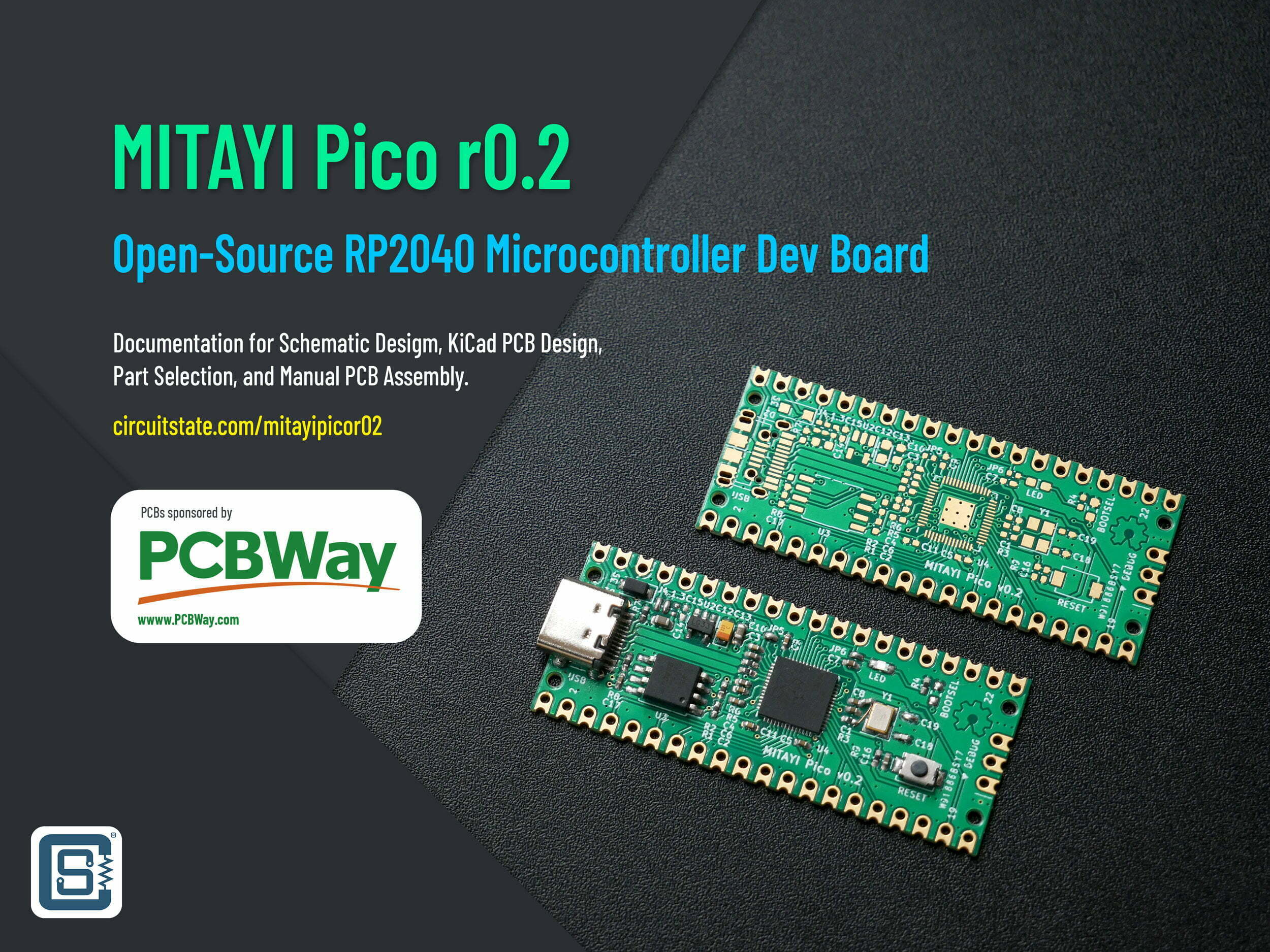
We have a dedicated post about the r0.2 design of Mitayi Pico RP2040 which you can find below.
MITAYI Pico RP2040 r0.2 – Open-source Microcontroller Development Board – Schematic, PCB and Assembly
Differences from Official RPi Pico
A quick comparison between the Mitayi Pico r0.5 and the official Raspberry Pi Pico board.
| Feature | Mitayi Pico r0.5 | Raspberry Pi Pico |
|---|---|---|
| USB | USB-C/USB-Micro | Only USB-Micro |
| Flash Memory | 16 MB, SOIC-8 package | 2 MB, USON-8 |
| Reset Button | Yes | No |
| Bootsel Button | Yes | Yes |
| Power LED | Yes | No |
| Debug LED | Yes | Yes |
| GPIO Pins | Breaks out all GPIO | Does not break out all pins |
| Voltage Regulator | 3.3V, 500 mA Linear LDO | 800 mA buck-boost switching regulator |
| Component Silkscreen Reference | No | No |
| Smallest component size | 0402 | 0201 |
| Completely Open-source? | Yes | No |
Schematic
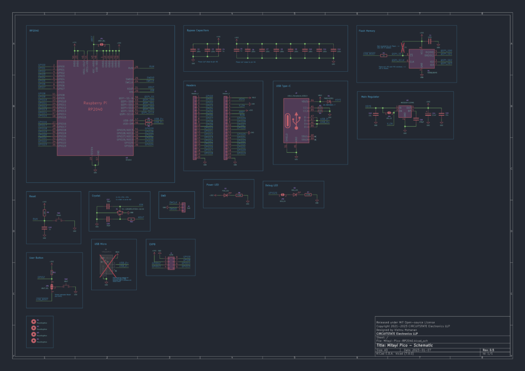
We explained the entire schematic design in the previous design documentation. But for the sake of completion of this post, we will explain everything again. The schematic was originally designed in KiCad V6 but as of writing this documentation, KiCad V7 has been released and we updated the files to the new versions. So you can’t open the V7 files with V6 anymore due to the breaking changes introduced in V7.
RP2040
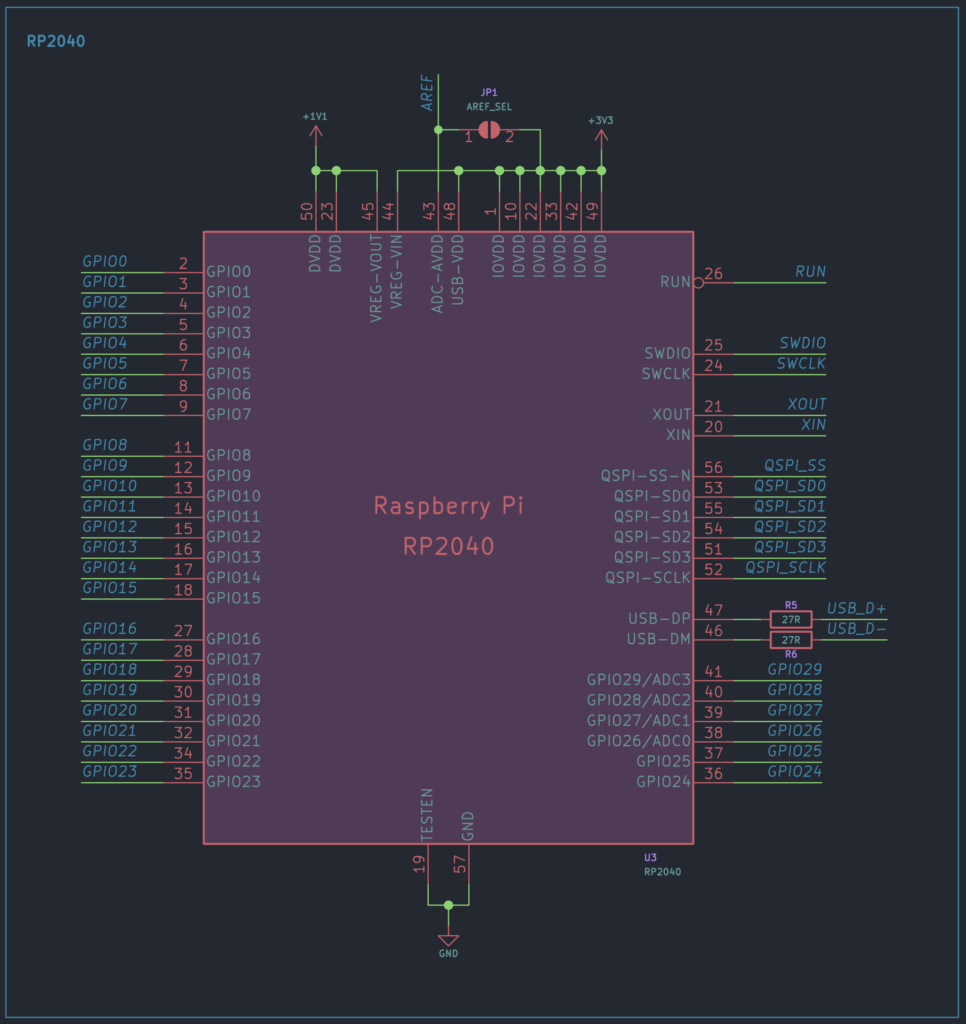
The schematic of the RP2040 microcontroller remains unchanged. RP2040 requires two different working voltages; 1.1V for the core and 3.3V for everything else. We do not need to supply both voltages. The RP2040 has an internal 1.1V low drop regulator (LDO). We need to supply +3.3V to all IOVDD pins and the VREG-IN pin. The VREG-IN is an input to the 1.1V LDO) and its output VREG-VOUT must be connected to all the DVDD pins. Additionally, we need to tie the 3.3V supply to the USB-VDD pin as well. The ADC-AVDD pin accepts the supply for the internal ADC. The ADC is very sensitive to supply noise, drift, and other interference. So if you want maximum accuracy with your ADC readings, you can use a separate low noise and high precision voltage reference dedicated for the ADC. In the official Pico schematic, there are current limiting resistors and a capacitor on the ADC-AVDD pin. In the Mitayi Pico r0.5 schematic, the pin is provided with a solder jumper so that you can connect the ADC-AVDD pin to the 3.3V supply or provide your own external reference. The USB data lines have a 27R resistor in series with them.
Flash Memory
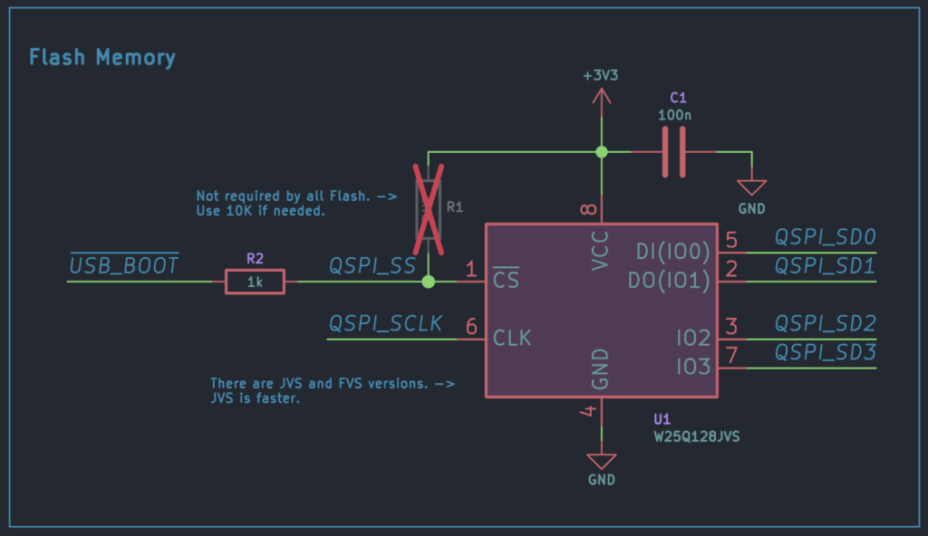
The flash memory we are using is the W25Q128JVSSIQ from Winbond in SOIC-8 package. The QSPI_SS (Chip Select) pin is connected to a push-button for putting the board into boot mode. In the previous design, we had a solder pad for the BOOTSEL function and that was a bad design choice. If the QSPI_SS pin is low when RP2040 boots up, the microcontroller automatically stops loading and executing any instructions from the flash chip. Instead, it will enumerate itself as a mass storage device (with the help of an on-chip Read-Only firmware), ready to accept new firmware. When we drag and drop a UF2 file to the drive, RP2040 will simply rewrite the flash memory with the new file and exit from the mass storage mode. The pull-up R1 is optional and should be 10K if used.
USB-C
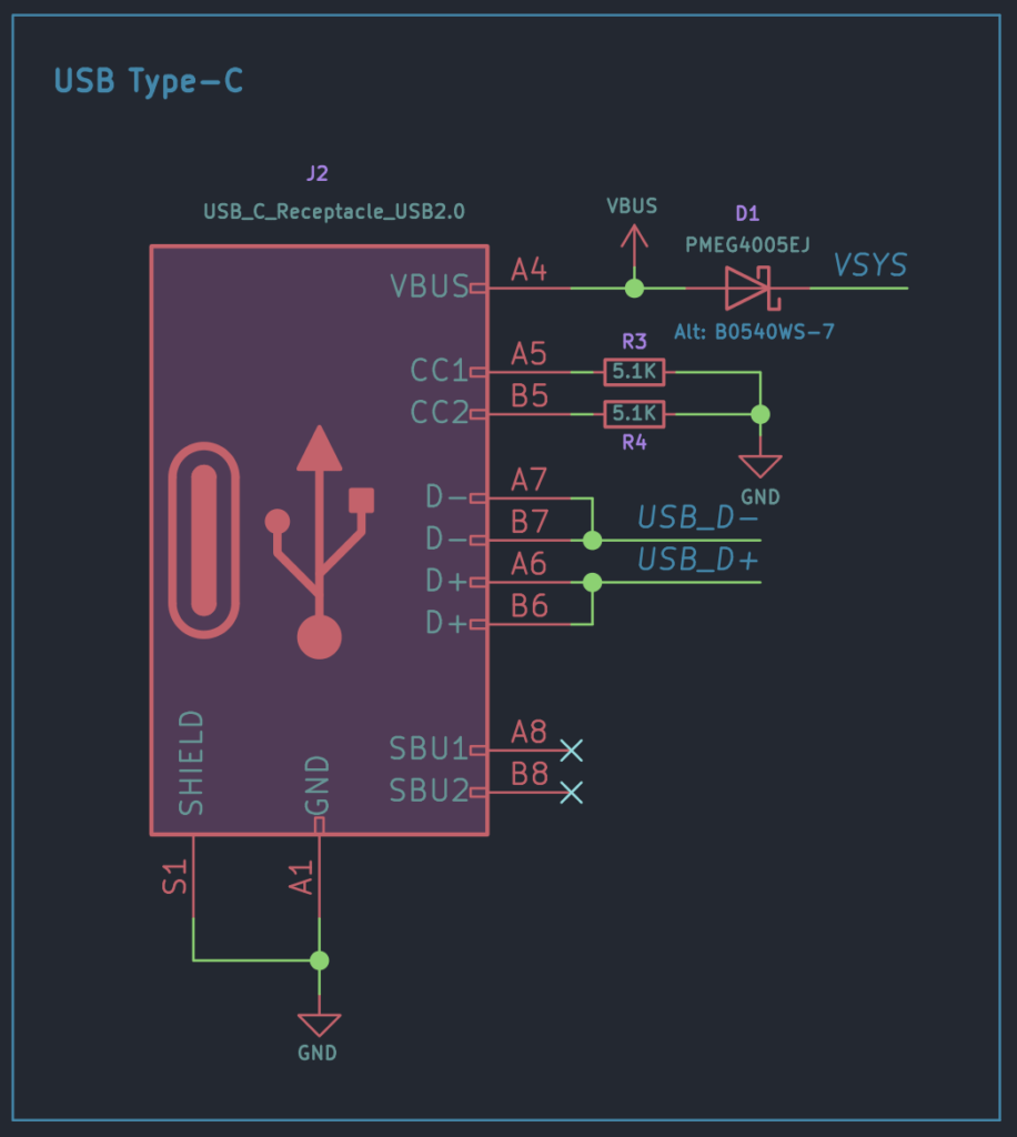
The USB schematic remains unchanged. We have both USB-Micro (MPN: Molex 105017-0001) and USB-C (MPN: Korean Hroparts TYPE-C-31-M-12) receptacle options in the Mitayi Pico r0.2 design. The USB-C receptacle is used as a USB 2.0 interface with two data pins (USB_D- and USB_D+) and two supply pins. The identical bus pins are tried together and connected to the USB pins of RP2040. The two 5.1K resistors on the CC1 and CC2 lines allow the USB device to be detected and do proper current sourcing. The auxiliary bus pins SBU1 and SBU2 are not needed and are thus not connected. The VBUS provides a 5V supply from the USB and it is connected to the 3.3V voltage regulator via the Schottky diode MBR1020VL. The diode protects the USB host from a reverse supply input.
Micro-USB
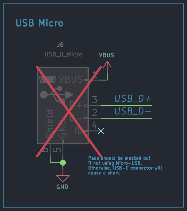
Stacking a USB-Micro and USB-C footprint on a PCB is possible and therefore we decided to keep both in the Mitayi Pico design. Even though USB-Micro is nearly outdated, the connector is still cheaper than a USB-C connector. So in case you want to use the USB-Micro as a fallback option, it’s there. We prefer USB-C for everything and so we have DNPed (Do Not Populate) USB-Micro. This is a new feature in KiCad V7. We can mark parts as DNP and they will be excluded from BoM, Assembly Files, etc. But the schematic symbols and footprints will still be retained. DNP components will be greyed out with a cross to better identify them. The new feature is different from the Exclude from Board option KiCad already had.
Main Voltage Regulator
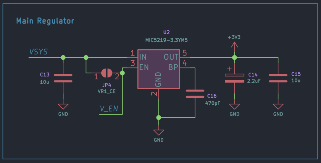
The main 3.3V regulator is an MIC5219-3.3YM5 from Microchip. It is an LDO with a maximum output current of 500 mA. The low drop means you can power the board from a 3.7 V Li-Ion or Li-Po battery directly. The VR1_CE is a solder jumper that you can use to enable/disable the voltage regulator and use the V_EN signal to turn the entire board ON/OFF with a digital signal. The C14 should be a Tantalum capacitor with 2.2uF or 4.7uF.
The previous design r0.2 had a few more solder jumpers and an extra AMS1117 voltage regulator. They have been removed from the r0.5 design.
Reset
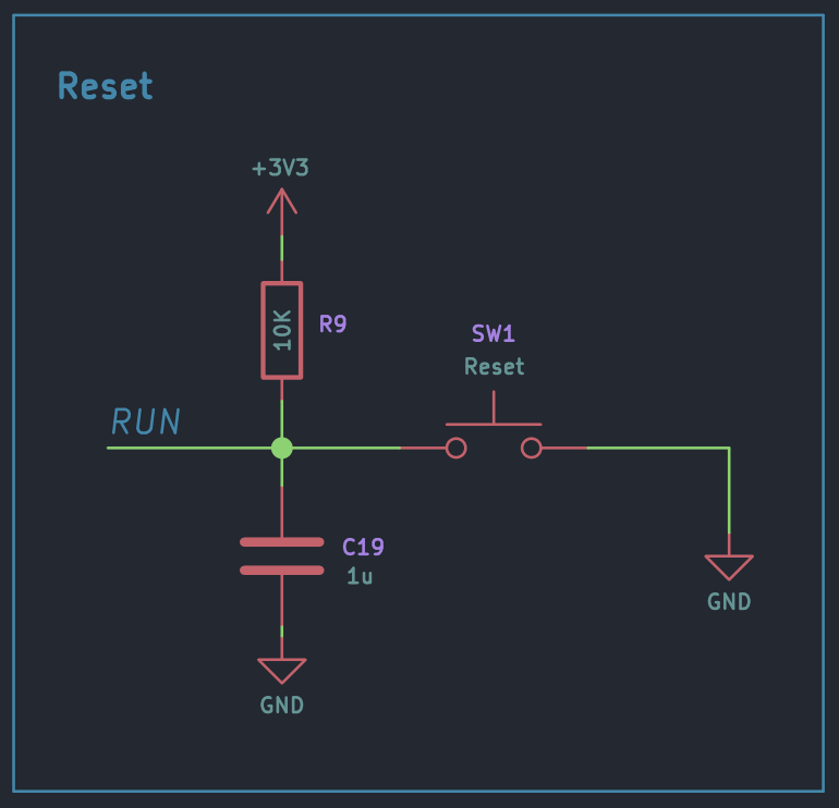
The reset function of the RP2040 is available as a push-button and as a pin. The official Pico does not have a dedicated push-button for resetting. For the push-button, we used a 2-pin SMD type usually found on ESP32 boards – 3x4x2mm SMD Tactile Switch.
BOOTSEL/User Button
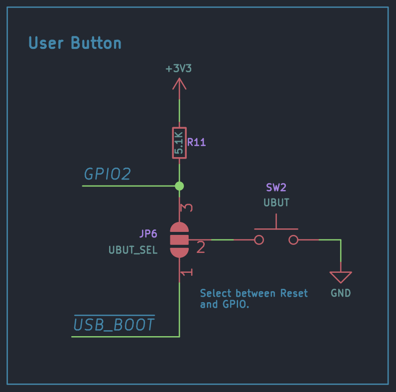
This is a new addition to the r0.5 design. Previously we only had a solder pad for the BOOTSEL function. That has been fixed. You only need the BOOTSEL button for putting the RP2040 microcontroller into program mode. Once the program is flashed, the remains unutilized. So we thought of adding a solder jumper to change the functionality of the BOOTSEL button to a custom user button connected to a GPIO pin. The BOOTSEL button is connected to GPIO2. By enabling the solder jumper, you can select one of the functions.
Crystal
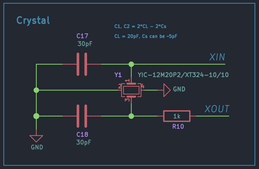
The schematic of the crystal in revision 0.2 was disastrous. I used the wrong schematic symbol and had to fix the issue on the PCB during assembly. It has been fixed in revision 0.5. We now have a 4-pin schematic symbol instead of a 2-pin one.
The crystal we are using is a 12 MHz SMD type – 12M20P2/XT324-10/10 from YIC. The 12M20P2/XT324-10/10 has a load capacitance of 20 pF and we need around 30 pF external capacitors to achieve that. You could also use capacitances close to that value such as 27 pF without any issues. The external capacitance value is calculated as,
C18, C19 = 2 * (CL - Cs)
CL = 20 pF, Cs can be ~5 pF
∴ C18, C19 = 2 * (20 - 5) = 30 pF
Debug LED
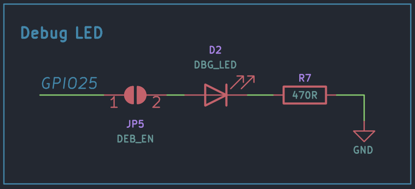
The debug LED is connected to GPIO25 through a solder jumper DEB_EN which allows you to disconnect the LED in case you need the pin for anything else.
Power LED
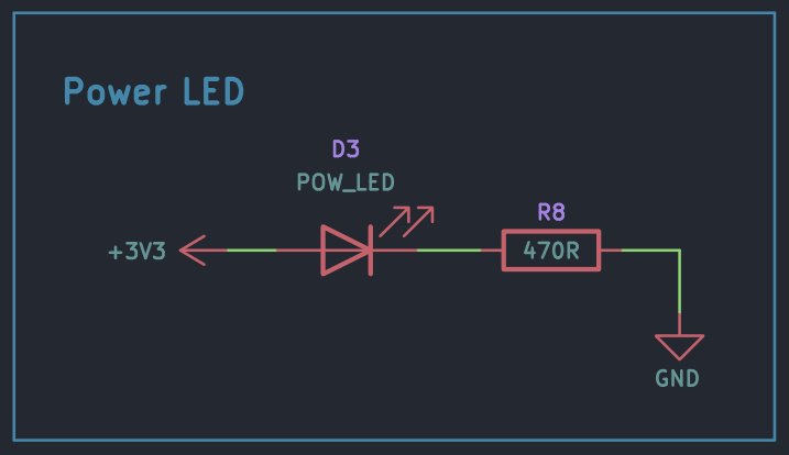
The power LED is connected to the 3.3V supply. The original Pico doesn’t have a power LED.
Pin Headers
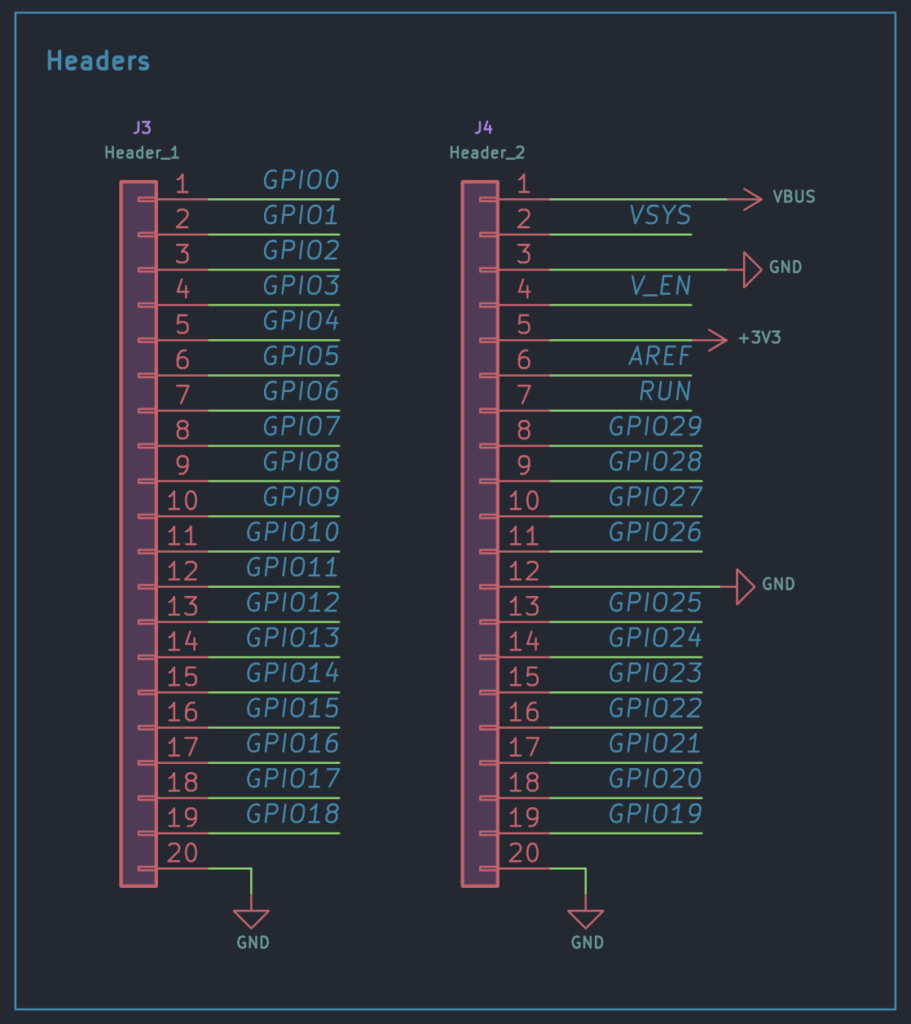
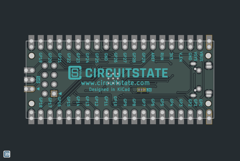
The two rows of pin headers break out all the GPIOs, power supply, and control pins. The official Pico does not break out all the GPIO pins. So to accommodate the extra pins, we had to break pin compatibility with the official board. But we have kept the power supply and control pins in their respective places.
SWD
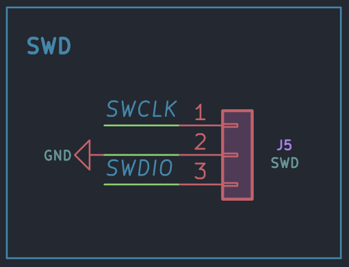
This is an SWD (Serial Wire Debug) connector with the pinout and position the same as the official Pico.
EXP8 Expansion Connector
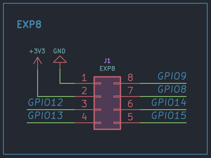
This is a new addition! The EXP8 is a new universal quick-expansion connector we plan to include in all future microcontroller board designs. EXP stands for “expansion” and 8 indicates the pin count. This is a standard 2.54 mm header pins 2 x 4 configuration. You can solder either the male or female versions of the header. The EXP8 on Mitayi Pico r0.5 breaks out at least one SPI, UART, and I2C. In the future, we can expand this connector as EXP10, EXP12, etc by adding more peripheral pins. The power pins will remain in the same place and that means you can still mate an EXP8 connector to an EXP10 without issues. The expansion connector is meant for adding extra functionalities to the development board such as Wi-Fi, SD card, etc.
Our initial plan was to make an 8-pin header compatible with the popular ESP8266 module. Unfortunately, the power pins are positioned diagonally on the connector and it prevented making the expansion connector interchangeable.
PCB Design
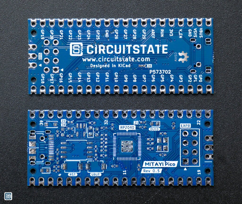
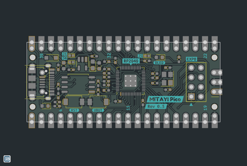
The PCB was designed in KiCad version 7. We opted for a 2-layer design so that manufacturing them can be easier. RP2040 was placed in the same orientation and almost the same location as the official Pico. The default track thickness and minimum clearance were 0.2 mm. All vias have the same size of 0.5mm/0.3mm (diameter/drill). For the pin headers with castellated holes, we simply modified a 20-pin pin header footprint with a 2.54 mm pitch. If the edge of the PCB goes through the center of a plated hole, it will create a castellated hole. The drilling/scoring should be precise and it needs some cleaning after.
The previous r0.2 design was fabricated by PCBWay with ENIG finish. But this time we used PCB Power, an Indian PCB manufacturer of high-quality multi-layer PCBs. Their prices are reasonable and they also provide component sourcing and PCB assembly services with excellent outputs. We opted for the HASL finish to keep the cost down. It has no impact on the assembly process or performance. Though we want to see the silkscreen quality improved. We got 5 PCBs with 10 days lead time for INR 2838.
We placed the push-button near the USB connector with a minimum spacing in between them. This allows you to use just a single finger to press and release the BOOTSEL (UBUT) and RESET (RST) buttons together to enable the program mode. If you look closer, you can see that we have masked out the USB-Micro footprint to prevent the USB-C connector body from shorting the USB signals which was an issue in the previous design. If you want to use a USB-Micro connector in place of USB-C, you will have to remove the solder mask layer from the pads.
The differential USB lines are no longer precisely impedance-matched. The official Pico and the Mitayi Pico r0.2 use proper impedance matching to allow the High-Speed USB to work at its full potential. In the r0.5 design, we just have regular differential line routing.
The OSHW emblem has been moved to the bottom side to make space for the EXP8 connector. The jumper J6 to select the function of the UBUT button is also on the bottom side.
Want professionally designed PCBs?
CIRCUITSTATE can turn your bare circuits into complex multi-layer PCBs with the highest performance and quality using industry-leading tools. We can also reverse-engineer your existing products to create accurate schematics and PCB layouts. Contact us today to share your requirements.
PCB Assembly
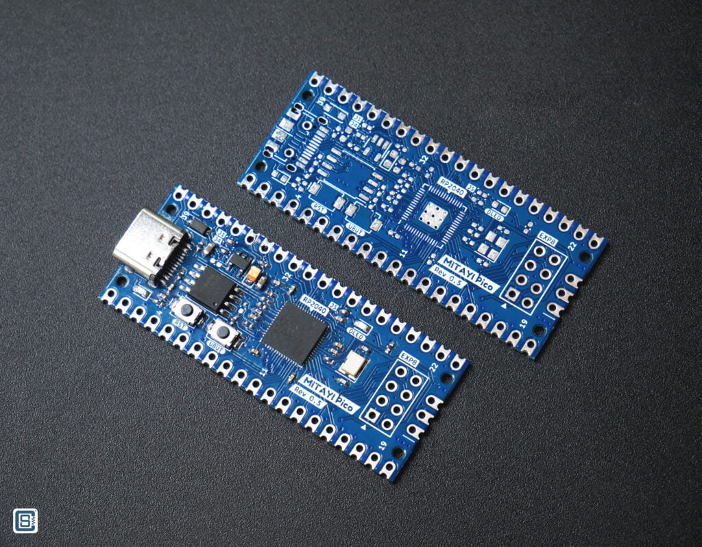
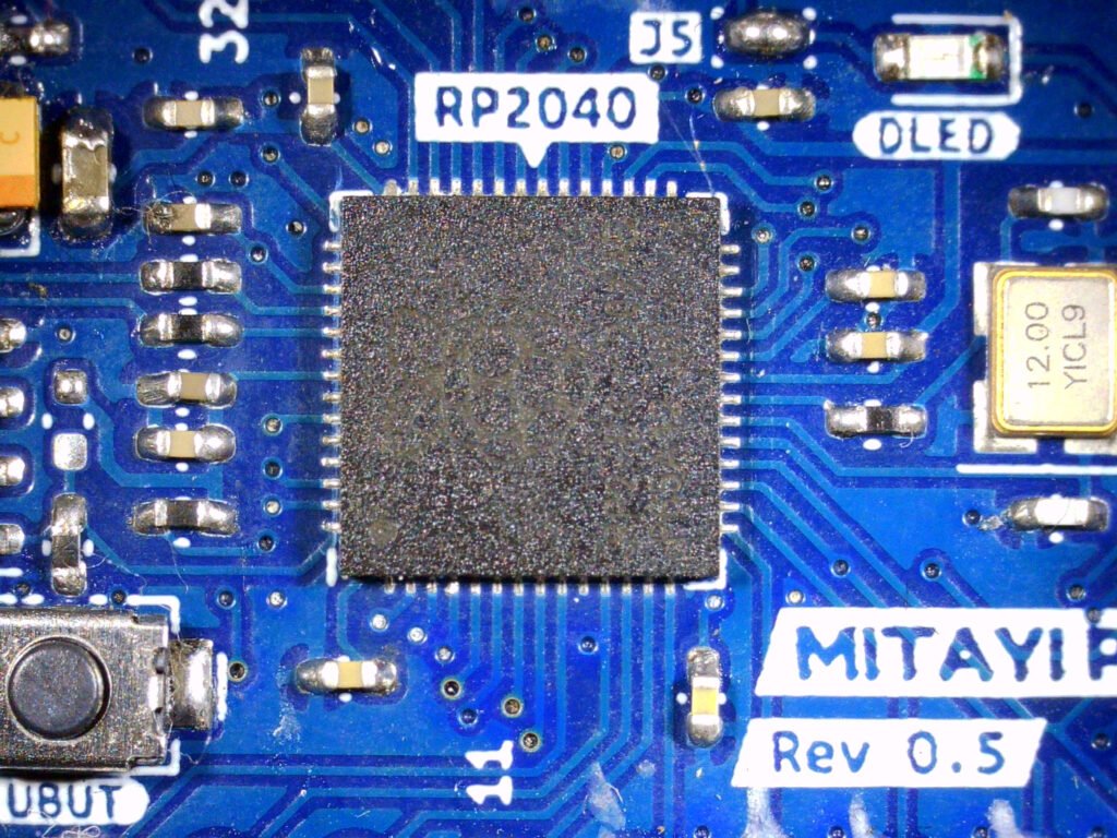
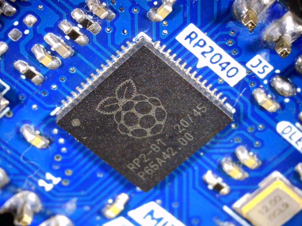
I assembled one PCB by hand for testing. To solder the crystal and the RP2040 I had to use a hot air blower. The remaining components were soldered with an adjustable soldering iron with 0.8D tip. I could not have soldered the RP2040 without the help from the digital microscope I bought recently.
Download
Links
- RP2040 Datasheet [PDF]
- RP2040 technical documentation
- Raspberry Pi Pico Datasheet [PDF]
- Hardware Design with RP2040 [PDF]
- Getting started with Raspberry Pi Pico [PDF]
- Minimal Design Example [ZIP]
- The VGA, SD card & audio demo boards for Raspberry Pi Pico and Raspberry Pi Pico [ZIP]
- Raspberry Pi Pico – High-Quality Pinout Diagram
- Getting Started with Raspberry Pi Pico : RP2040 Microcontroller Board – Pinout, Schematic and Programming Tutorial
- RP2040 and Pico: All New Microcontroller and Development Board from Raspberry Pi
Short Link
- Short URL to this page – https://circuitstate.com/mitayipicor05
