Wiring Up & Writing Your First Blink Program Using Assembly Language : Learn Microcontroller with STM8S – Tutorial Part #4
Learn how to write your first Assembly language program for the STM8 microcontroller using the STM8 instruction set and blink and LED.
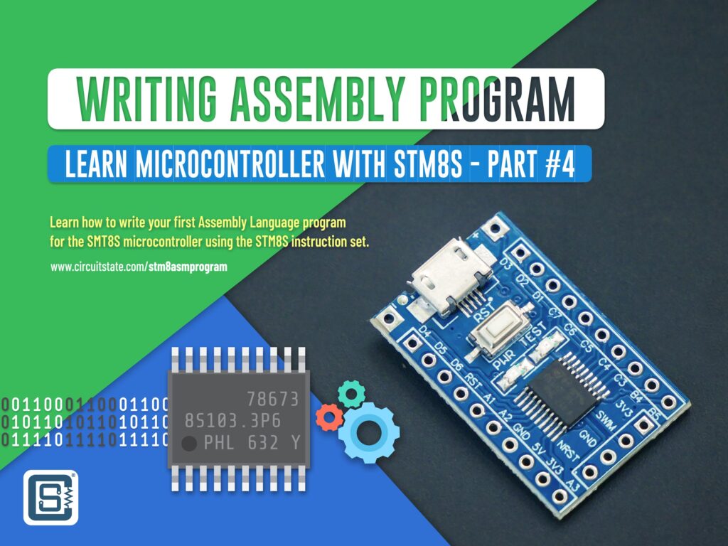
In the last tutorial, we laid the groundwork for writing our first Assembly language program for the STM8S103F3P6 microcontroller. In this tutorial, we will a do a lot of things with what we have learned so far. By the end of this tutorial, you will have programmed your first computer. We hope the pace of the tutorial is fine for you. Enough preface, we have a tutorial to complete. If you couldn’t catch up with the previous tutorial, you can do it now.
Installing Development Tools : Learn Microcontroller with STM8S – Tutorial Part #3
Tutorial Series
- Learn the fundamentals of microcontrollers.
- Familiarize with a simple STM8S microcontroller.
- Install all the software tools and prepare your computer for programming and debugging microcontrollers.
- Get hands on experience with connecting your first microcontroller board and write a program for it.
- Learn the concepts of timers and interrupts in microcontrollers and blink an LED with what you learn.
- Learn how to make your microcontroller interact with the world by reading a push-button.
- Learn how to read a push-button using external interrupts without blocking critical code.
- Learn how to use the UART peripheral to print your first “Hello World” message to a computer.
What You’ll Learn
- How to power-up your STM8S-Blue board.
- How to create your first Assembly language program for the STM8S.
- Basics of an Assembly language program.
- Basics of the STM8 microcontroller instruction set.
- Basics of microcontroller GPIOs and how to blink and LED.
- How to compile and upload code to the STM8S-Blue board.
- How to disassemble and analyse machine code.
Powering Up
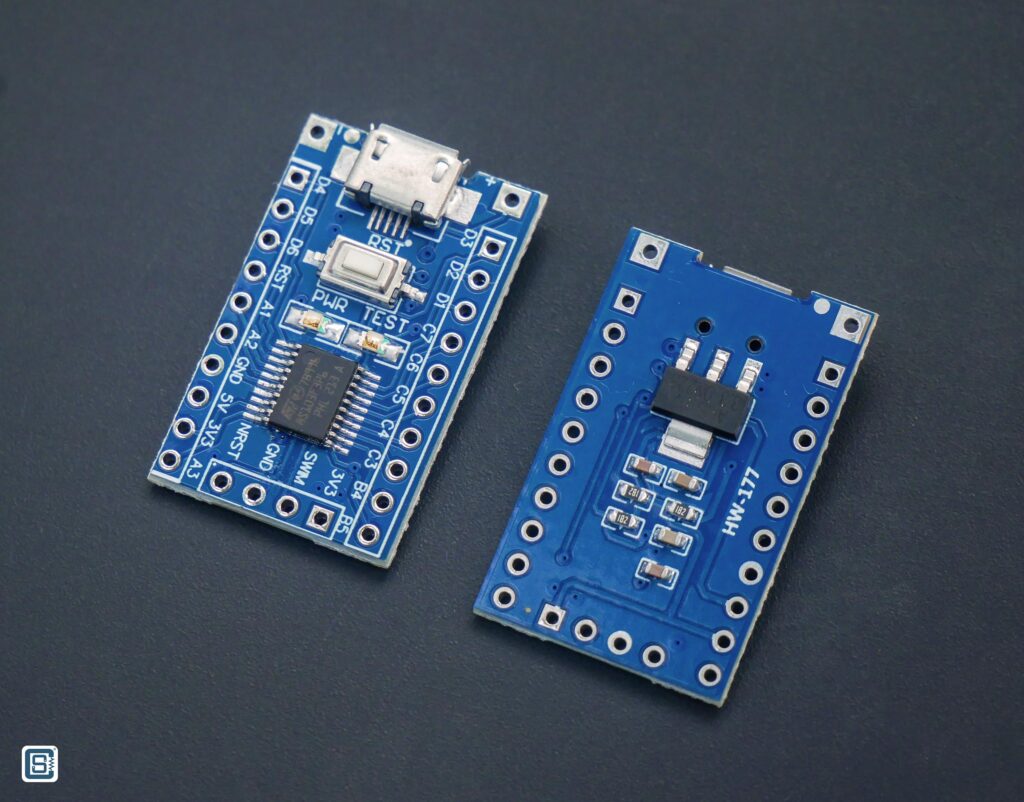
There are multiple ways to power up your STM8-Blue board. The easiest way is to connect your board to a PC or any other USB power source using a USB-Micro cable. You can also connect a 5V power supply using the two pads near the USB connector. When first powered up, you might see the TEST LED blinking. This is because of the program that is already running in the microcontroller. Factories might use an LED blinking program to verify that the board is working. But if the LED is not blinking, don’t worry, we will make it blink 😉
ST-Link Debugger
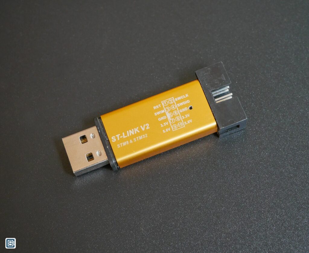
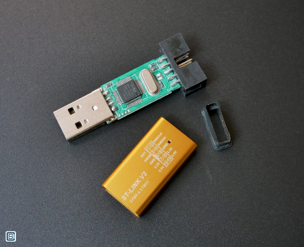
You should also have the ST-Link V2 debugger. If you bought it for around INR 300, then it is probably a clone. Official ST-Link programmers cost much more than that. Surprisingly, the clones just work in most cases and that’s all what you need.
Beware of one thing though; there are multiple variants of the ST-Link V2 debugger available from the online marketplaces. Some of them have conflicting pinouts. Just make sure to check the pinout printed on the debugger before connecting it to your board.
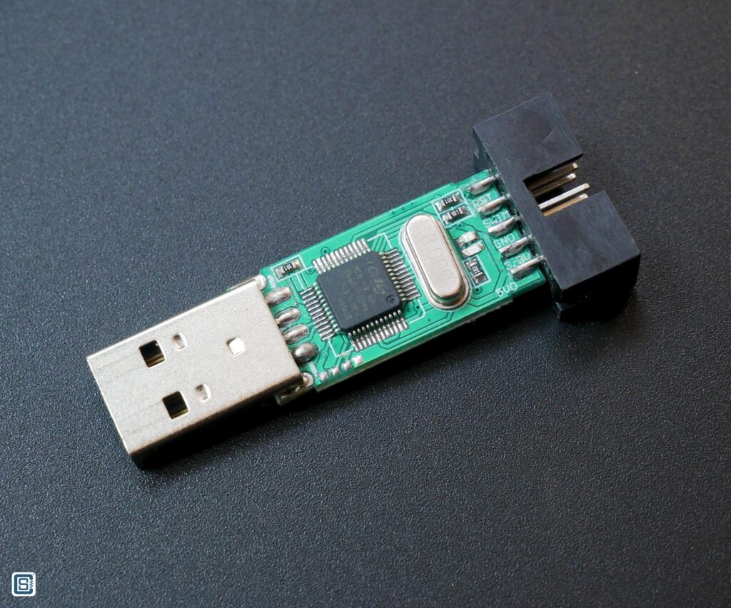
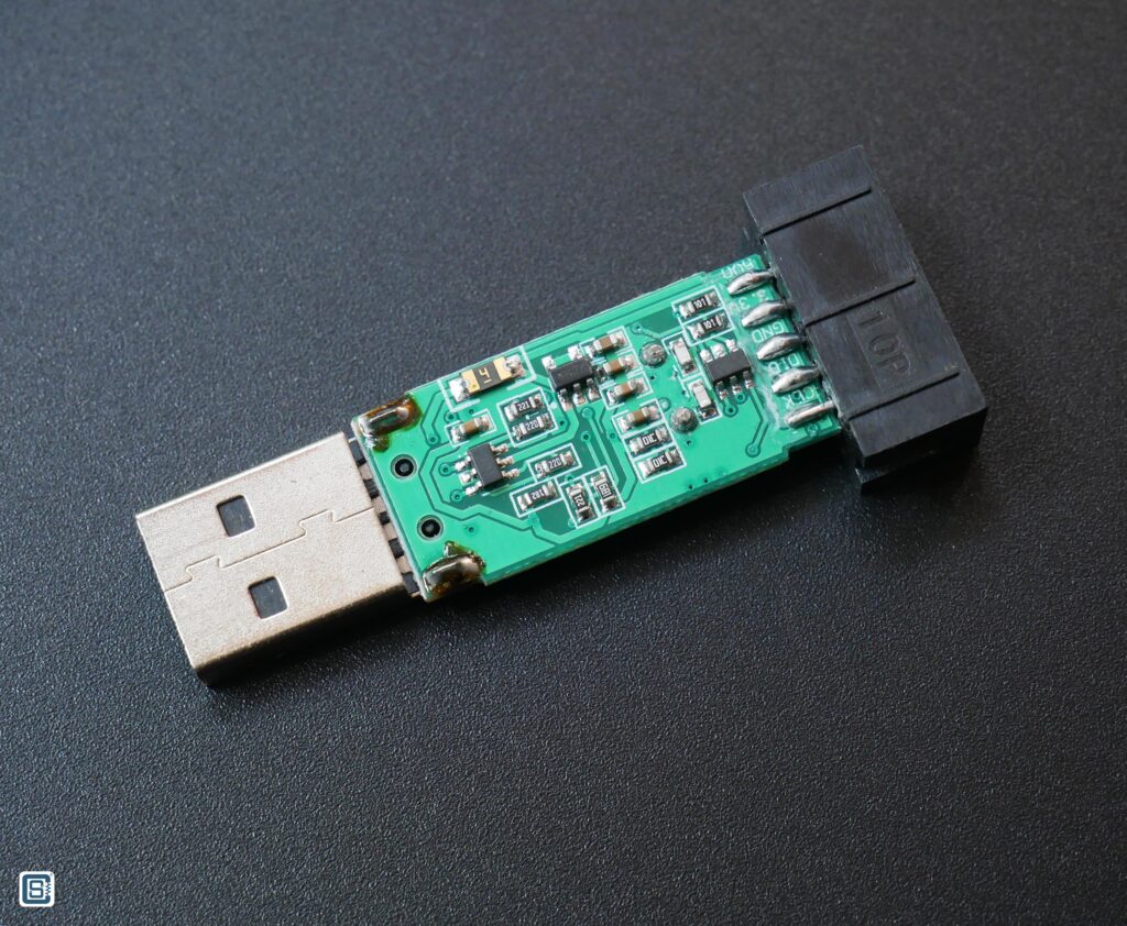
The arrow mark on the black connector indicates the first pin. Using the first pin marker, you can identify all other pins. The body of the debugger is made of Aluminium. Sometimes, the body can come in contact with the board and create issues. In that case, wrap the board with some Kapton tape to prevent it from touching the body.
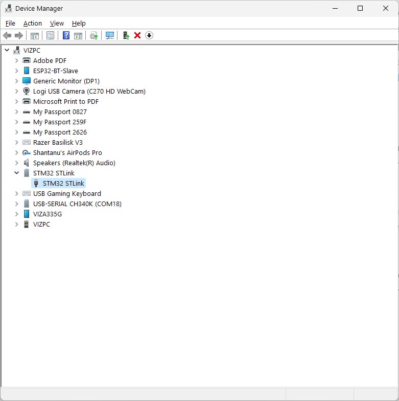
When you first connect the debugger, the device should automatically enumerate and appear as STM32 STLink on the device manager. The driver for the debugger is already installed when you installed the STVP tool. If the debugger does not show up the device manager, try running the installer again and click Yes to all of the driver installation prompts.
GPIO Basics
We already know that the TEST LED is connected to the PB5 digital pin of the microcontroller. We will learn how to turn this pin ON/OFF and blink the TEST LED. But before that, you should know a few things about the General Purpose Input Output (GPIO) pins.
Features
Following are the general features of the GPIO pins of the STM8S microcontroller.
- Port bits can be configured individually.
- Selectable input modes: floating input or input with pull-up.
- Selectable output modes: push-pull output or pseudo-open-drain.
- Separate registers for data input and output.
- External interrupts can be enabled and disabled individually.
- Output slope control for reduced EMC noise.
- Alternate function I/Os for on-chip peripherals.
- Input Schmitt trigger can be disabled on analog inputs for reduced power consumption.
- Read-modify-write possible on data output latch.
- 5 V-tolerant inputs.
- I/O state guaranteed in voltage range 1.6V to VDDIOmax.
Pins & Ports
A GPIO pin is a physical pin on a microcontroller that can be programmed to be in two logical states; digital HIGH or digital LOW. When in HIGH state, the voltage on the pin will be whatever the VDDIO (VDD I/O) voltage is. In the case of STM8S with a 3.3V IO voltage, the voltage at the pin will be 3.3V. When the pin is programmed to be in the LOW state, the voltage will be 0V. The state of the pin is controlled by a GPIO register. Since memory in a computer is organized in group of 8 bits, the GPIO registers are also 8-bit wide. This allows grouping of up to 8 GPIO pins on a single register. Each of the bit on the register will correspond to a single GPIO pin.
In microcontroller terminology, each group of pins are called ports. The STM8S103F3P6 has four such ports named A, B, C and D. Each port has 8 GPIO pins in them and therefore the total number of pins can be 32. But not all of these pins are broken out of the microcontroller. You can check the pinout of the STM8S103F3P6 to see which pins are available.
The GPIO pins are named with the port name and the position of it in the register. For example, the first pin of Port A is called PA0. Notice that the GPIO number starts at 0 instead of 1, just like how the bit positions on a register are expressed. So the last pin of the Port A will be called PA7, and not PA8. Keep that in mind.
Port Registers
In addition to the GPIO functions, a GPIO pin can also be assigned with alternate functions such as ADC input, communication interface etc. These functions are determined by extra registers. We also need to tell the microcontroller which GPIO function we need. We need to explicitly set a pin to Output mode to make it LOW or HIGH from the program. If we want to accept an input through a GPIO pin, for example from a push-button, we need to set it as an Input. Following are the types of GPIO port registers available on the STM8S.
- Data Direction Registers (DDR) – these registers determine if a GPIO pin should be Input or Output. Each port has a single DDR register associated with it denoted as
Px_DDR. For example, for Port A, this will bePA_DDR. You can mix up different modes for different GPIO pins on the same port. DDR registers are read-write enabled. - Data Registers (DR) – these registers hold the actual state of the GPIO pins. There are two types of DRs in STM8S.
- Input Data Register (IDR) – When the pin is in Input mode, this register will hold the input state of the pin. The register is denoted as
Px_IDR. For example,PA_IDR. The input registers are read-only, and any write to them are ignored. - Output Data Register (ODR) – When the pin is in Output mode, the data in the DR register will hold the output state of the GPIO pin. The register is denoted as
Px_ODR. For example,PA_ODR. Output registers and read-write enabled. You can write to the pin, and also read the state back.
- Input Data Register (IDR) – When the pin is in Input mode, this register will hold the input state of the pin. The register is denoted as
- Control Registers – these registers determine the alternate functions and other properties of the GPIO pins. There are two sets of control registers for all of the ports.
Px_CR1andPx_CR2.
To make a GPIO pin LOW, we just have to write that corresponding bit in the ODR register with binary 0. Similarly, to make the GPIO pin HIGH, we can write a binary 1 to it. But in order to write digital states to a GPIO pin, we must set its function as an Output. We can use the DDR register to set that. Pins set as Input can not be driven like this. The microcontroller will simply ignore our commands. We will learn how to use these registers when we write the programs. If we explain it now, it will only confuse you. Let’s cover the basics first.
Pin States
When you start learning about GPIO pins, you will often hear terms like floating, pull-up, pull-down etc. These indicate the state of the pins at a given time. Since these terms can be confusing to you, we should explain them at this point.
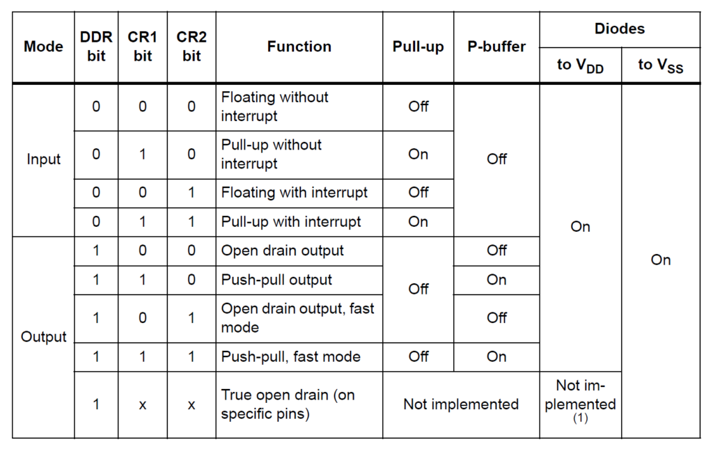
Input Modes
When a GPIO pin is set to an Input and nothing is connected to it, the state of the pin is referred to as floating. This means, the voltage level of the pin is not determined. It can randomly change to different states. Floating pins are usually a bad thing when designing microcontroller systems. We want all of the pins to be in some known state.
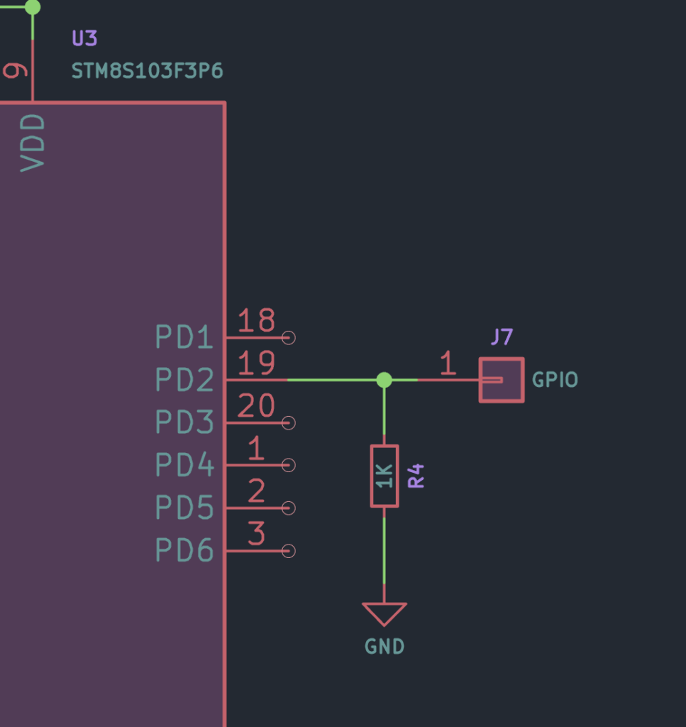
To prevent a pin from floating, we can connect it to a logical HIGH voltage or a LOW voltage. This is usually accomplished with the help of pull-up resistors and pull-down resistors. A pull-up is a large value resistor that connects a GPIO pin to the logical HIGH voltage. On the other hand, a pull-down resistor a large value resistor that connects a GPIO pin to the logical LOW voltage.
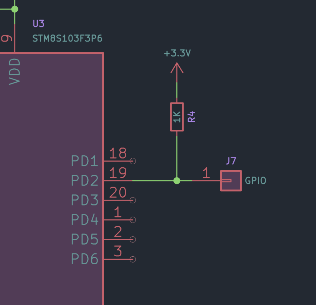
But why are we using resistors here, can’t we just connect the pins directly to the supply voltage or GND? Check the following simple circuit. The input GPIO pin is connected to the positive voltage to prevent it from floating. An SPST (Single-Pole Single-Throw) push-button is also connected to the pin. When we press the button, it connects the GPIO pin to the GND and asserts a logical LOW on the pin. Or that we would expect. Instead, you will simply short the positive and negative supply pins which is bad.
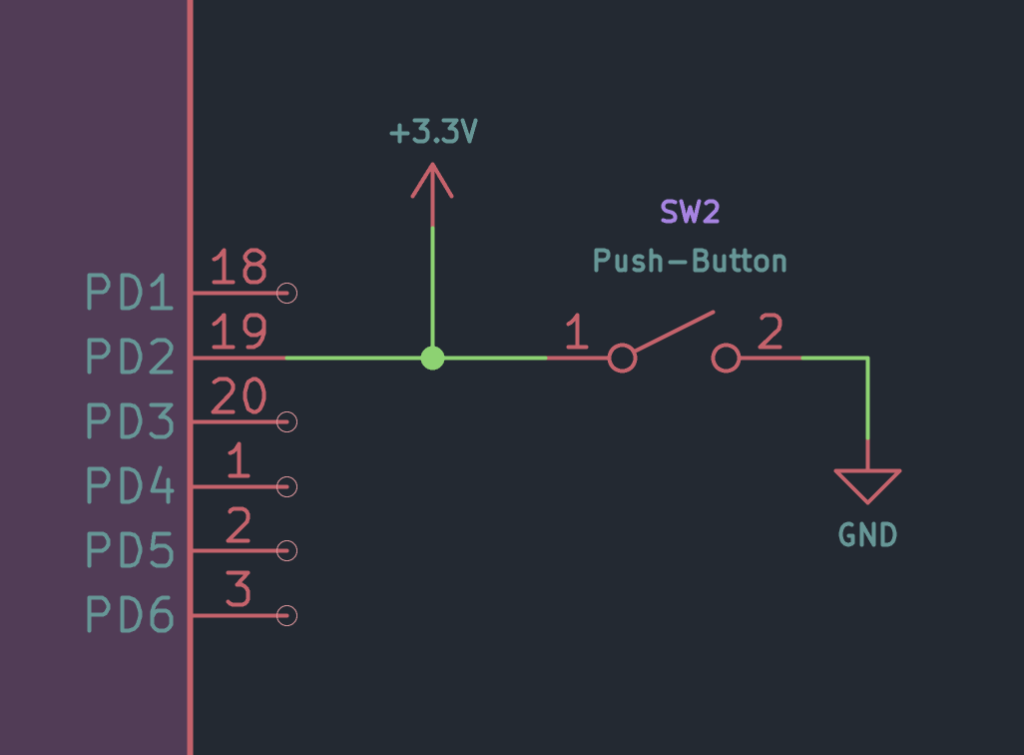
So what about adding a series resistor to limit the current? If we add it, we will solve the shorting problem but pressing the button will generate only a weak pull-down.
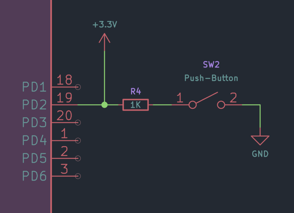
The solution is to add a large value resistor from the GPIO pin to the positive supply. Since the value of the resistor is large, it does not draw much current but is still able to “pull” the the pin to a known state. When the push-button is pressed, the pulled up voltage is overridden by the strong GND voltage and thus asserting a logical LOW state on the pin. This solves all of the problems we had.
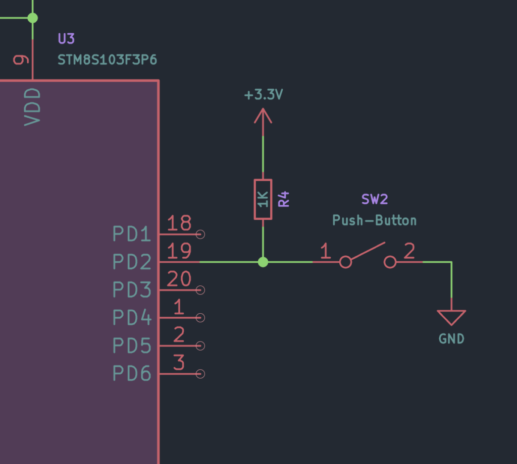
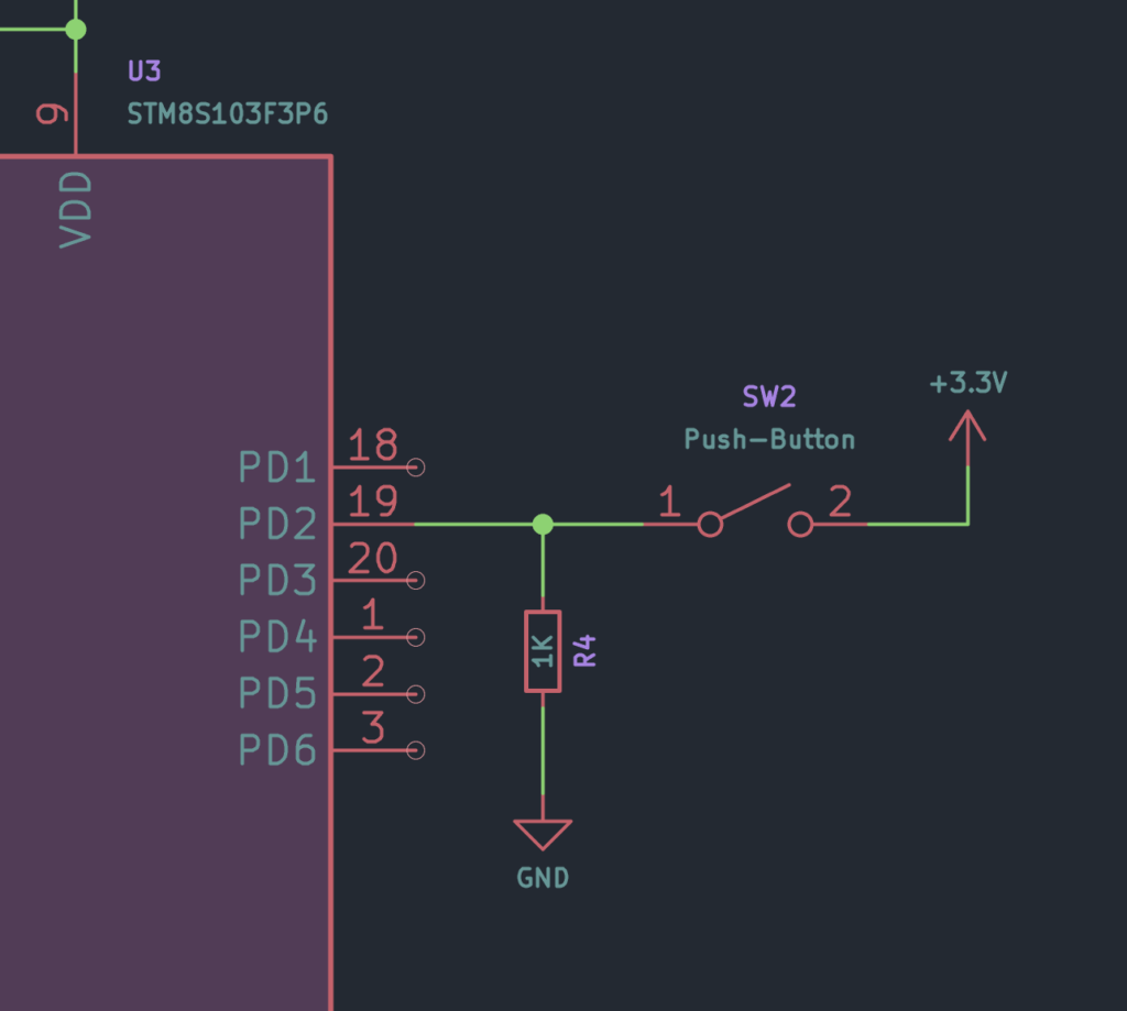
LOW on the GPIO pin.Similar to a pull-up, a pull-down is also possible in the following configuration. In this case, when we press the push-button, we will assert a logical HIGH to the pin. Whether to use a pull-up or a pull-down on a GPIO pin is application specific.
Output Modes
When a GPIO pin is set to an Output, it can stay in two modes; push-pull mode and a pseudo open-drain mode. The push-pull mode is where a pin can be driven either to the VDDIO voltage or the GND voltage, with either sourcing or sinking current respectively. There is a limit to how much current each GPIO pin can sink/source which will be specified in the datasheet. You have to make sure that you don’t exceed this rating.
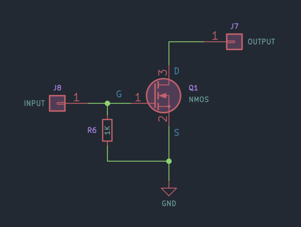
An open-drain output refers to when the Drain pin of an output Mosfet is left floating. At this time, the Source pin of the Mosfet will be connected to the GND potential. So when the Mosfet is turned on, any load that is connected to the Drain pin will be connected to the GND. But why is this important? One advantage of having an open-drain output is that, you can pull-up the pin externally to a larger voltage than the VDDIO voltage. There can be cases when this is useful. Pulling up an open-drain pin to a voltage higher than the VDDIO voltage will not damage the MCU. Most of the GPIO pins on STM8S are pseudo open-drain because of the presence of protection diodes that connects to VDDIO and the GND as you can see from the diagram below. Only the I2C pins PB4 and PB5 are truly open-drain in which the diodes are not implemented. These pins are marked T in the pinout diagram.
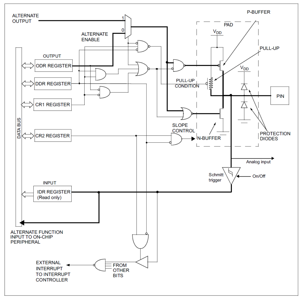
PB4 & PB5). Source: ST MicroelectronicsThe GPIO pins on the STM8S pack a few more features in addition to the simple outputs and inputs. You can adjust the maximum speed at which you can switch the GPIO pins by adjusting the slew-rate, accept interrupt signals, and filter the input through a Schmitt trigger. The best place to find more details on all of these is the official STM8S Series Reference Manual. We will explain more of the functions of the GPIO pins on the fly.
Assembly Language
By now, you already know that we need to provide instructions and data for a microprocessor/microcontroller to do computation. In the earlier days, the instructions and data to the computer were given through various switches and knobs by the human operators. This is just like inputting values on a calculator and doing the calculations on them. At one point, we figured out that instead of manually providing the inputs every time, we can simply store the instructions and data in some reusable medium and make the computer read the medium sequentially. One example of an early type of storage is Punched Cards. Even though we no longer use punched cards for computers, the idea of reading a medium for instructions and data remains the same. The medium we are using today are faster and compact electronic storage media.
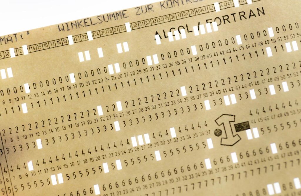
But it still begs one question. What format do we use to write the instructions and data? As we know, any data can be converted and stored as Bits (binary digits) on an electronic storage media, what we generally call the memory. The style and conventions we use to write the instructions and data for a computer form a soft language generally referred to as Assembly Language. Assembly language is not single exclusive language, but a loose term for different conventions used for writing instructions for different CPUs. So no two Assembly language programs need to be the same.
Since the process of writing instructions in binary format and conveying them can be very difficult between people, we developed placeholders for each instructions and we now call Mnemonics (M is silent). For example, the mnemonic MOV is generally used for the data move instruction. The instruction asks the CPU to move data from one memory location to another. The way a specific CPU architecture executes this operation can be different from another kind of CPU, but the concept remains the same. Every CPU we use today are finite state machines with a finite set of instructions. The finite set of instructions accepted by a CPU is called the Instruction Set of that computer. Even though the number of instructions are limited in number, we can carry out any complex operations with a set of them. In other words, using a finite instruction set, we can write infinitely many and infinitely long programs to accomplish any type of calculations.
STM8 Instruction Set
An 8-bit CPU can have up to 256 (28) instructions. The STM8S has 96 instructions that can be logically classified into 13 groups as shown below. As we said earlier, these instructions are denoted by their mnemonics and each mnemonic has a corresponding binary value which is called an Op-Code (Operation Code).
For example, the NOP instruction is the most simplest instruction you can find. It stands for No Operation, and when it is executed the CPU does nothing and waits for the next instruction. The NOP instruction finds use in implementing delays between instructions. The op-code of the NOP instruction is 0x9D in hexadecimal format (0x indicates hex number), 157 in decimal, and 0b10011101 in binary (0b indicates binary). Throughout this tutorial, we will use the hexadecimal representation of the op-codes. Below is a table of the STM8 instruction set.
| Load and Transfer | LD | LDF | CLR | MOV | EXG | LDW | CLRW | EXGW | EXGW | EXGW | EXGW |
|---|---|---|---|---|---|---|---|---|---|---|---|
| Stack operation | PUSH | POP | PUSHW | POPW | |||||||
| Increment /Decrement | INC | DEC | INCW | DECW | |||||||
| Compare and Tests | CP | TNZ | BCP | CPW | TNZW | ||||||
| Logical operations | AND | OR | XOR | CPL | CPLW | ||||||
| Bit Operation | BSET | BRES | BCPL | BCCM | |||||||
| Conditional Bit Test and Branch | BTJT | BTJF | |||||||||
| Arithmetic operations | NEG | ADC | ADD | SUB | SBC | MUL | DIV | DIVW | NEGW | ADDW | SUBW |
| Shift and Rotates | SLL | SRL | SRA | RLC | RRC | SWAP | SLLW | SRLW | SRAW | RLCW | RRCW |
| SWAP | RLWA | RRWA | |||||||||
| Unconditional Jump or Call | JRA | JRT | JRF | JP | JPF | CALL | CALLR | CALLF | RET | RETF | NOP |
| Conditional Branch / Execution | JRxx | WFE | |||||||||
| Interrupt management | TRAP | WFI | HALT | IRET | |||||||
| Condition Code Flag modification | SIM | RIM | SCF | RCF | CCF | RVF | |||||
| Breakpoint /software break | BREAK |
Before we can start writing our first Assembly language program, we need to learn a few basic things about the language. To not overload you with so much information at this point, we will keep everything brief here.
Addressing Modes
Part of telling the CPU to execute an instruction is specifying how to access the memory. Yes, there are more than one ways for accessing the memory and the methods are called Addressing Modes. The most straight forward method is to specify the address of the memory location and the CPU will directly access it. This method is usually referred to as Absolute Addressing Mode. With such a method, we can ask the CPU read a location anywhere on the memory. Another method is to specify a common starting point and then specify an offset of number of memory locations. This is called Relative Addressing Mode. It avoids the need to individually specifying all memory addresses, and keeps the program efficient. Yet another method is the Immediate Addressing Mode, in which the location is right next to the instruction. This allows combining data along with the instructions. What we explained so far are a few of the common addressing modes. But there can be more. We will learn about all of them when we explain the programs.
Pre-Codes
As we said earlier, an 8-bit CPU can have up to 256 single byte instructions. So where are the remaining ones after the 96? Well, too many unique instructions can be very impractical for a programming language. So instead of having 100s of op-codes, we can modify some of the existing instructions using extra op-codes. In the STM8S, we have single byte pre-codes which are op-codes that come just before a regular instruction. A pre-code can tell the instruction decoder how to decode the next instruction. This adds a modularity in the program which translates to more maintainable code. We will see how the pre-codes are used in the upcoming examples.
Operands
Similar to how op-codes represent instructions, the data for the instructions are called operands. They are data supplied along with the instructions. That said, there are instructions that does not accept operand from the programmer but still does something useful. This is because there are two ways the operands are specified. In the Explicit mode, the operands follow the instructions in the program memory. That means, without the operands, the instruction will fail to execute. In Implicit mode, some instructions are designed only to work on operands located in specific places, that we do not need to tell the CPU where to get the data from. Such instructions do not require the operand to be specified.
CPU Registers
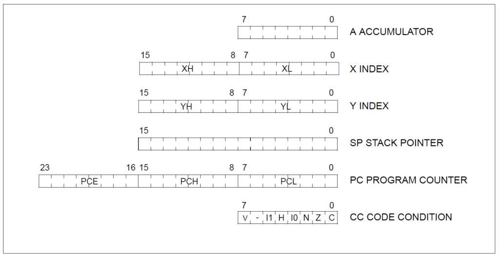
CPU registers are fast-accessible memory locations tied to the CPU itself. The inputs (instructions & data) and the outputs (data) from the CPU are stored in the CPU registers. There are only a handful of them as shown in the picture below.
Accumulator
Accumulator, shorthanded as A, is the core register that holds the operands as well the results of arithmetic and logic operations. It is an 8-bit register and therefore can only store a single byte at a time. That also means, if the result is ever greater than a byte can hold, we need a mechanism to handle that, which we will learn about shortly. The size of the accumulator usually determines the bit-width of a microprocessor. STM8S is an 8-bit microcontroller because its ALU and the Accumulator are 8-bit in size.
Index Registers
There are two 16-bit index registers, X and Y. Since they have two bytes each, each of the byte can be denoted as a high register (H) and low register (L). For X register, this is XH and XL. Similarly, for Y register, these are YH and YL. These registers can be accessed as individual bytes or as a 16-bit value. The index registers are generally used to specify memory locations, and while they are not busy with that task, you can use them as general purpose registers.
Stack Pointer
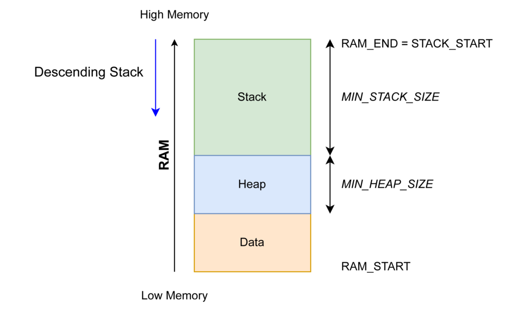
A stack in computing, is a unique way of using memory for programs. It is a Last-In First-Out (LIFO) method of accessing the memory. Suppose you are washing plates and stacking them on top of one another. The last plate you washed will be the first one to be used from that stack. And the first plate will be taken out at the end. A stack memory is accessed the same way.
But why does this matter? We know that we can use simple CPU instructions to write complex programs, even without using an infinite number of instructions. When we do that, we take advantage of a concept called a subroutine (also called function) to efficiently write programs. A subroutine is simply a group of instructions that can be reused in many places in the program instead of writing the instructions everywhere when we need them. When the program flow switches from the main program to the subroutine, whatever values exist on the CPU registers need to be stored somewhere, so that the subroutine can use the CPU registers. But after the subroutine is complete, the program flow must go back to the main program and restore the contents of the CPU register back to their old values. Now you are getting why we are using a LIFO method for accessing the stack. The state of the CPU registers at a particular state of the program is called a context. When the context switching happens, for example when a subroutine is called, the stack takes care of efficiently saving and restoring the context.
Stack Pointer holds the address of the next free location on the stack. When the MCU is reset, the value of the SP is set to the upper limit, which means the largest memory address. When data is added to the stack, a process called pushing, the value of the SP is decremented by how many bytes have been pushed. So if two bytes are pushed to the stack, then SP is decremented by two. Similarly, when data is restored from the stack, a process called popping, the value of SP is incremented. When the value of SP reaches its lower limit, the value wraps around to the upper stack limit. Therefore, further pushing of data to the stack will overwrite the old values in the stack and result in a stack overflow error.
Program Counter
The Program Counter (PC) is a 24-bit (3 bytes) register that holds the memory location of the next instruction to be executed. Note that PC does not store the instruction, but a memory address. The instructions have to be somewhere in the memory. The CPU gets the next instruction from the location pointed by the PC. Since PC is 24-bit, it can access a memory space of maximum 16 Mebibytes (MiB). If you are wondering how,
224 = 16777216 Bytes
    = 16777216 / 1024 = 16384 Kibibytes
    = 16384 / 1024 = 16 Mebibytes
But why is the PC 24-bit, why not 16-bit or 8-bit? Well, having more memory space is always a good thing and 16-bit PC is a plausible size for tiny microcontrollers. 8-bit would be too small to do anything at all. So a sweet spot is selected for the size for the PC, to have enough address space but not too large for regular operations.
When the MCU is reset, the PC is loaded with the value in the RESET vector table. A vector table is simply a list of memory locations saved in the memory itself. The memory locations will point to different parts of the program in the memory. Therefore, when the MCU is reset the CPU loads the instruction pointed by the PC and starts executing it. After each instruction is executed, the PC is incremented to point to the location of the next instruction. This happens automatically, which also means, you as a programmer can not directly write anything to the PC. Program Counter has three bytes, PCL, PCH and PCE, in the order of significance.
Condition Code
The Condition Code (CC) register is where the state of the CPU is stored. Remember the case of carry forward when adding two large numbers than a byte can hold? Such conditions can be indicated by toggling bits in the CC register. Each such bit is called a flag. CC register is 8-bit wide and it holds 6 flags. The 6th bit is reserved and will always be 0.
Overflow
The Overflow (V) flag indicates a bit overflow when doing signed arithmetic operations. Since signed numbers are represented in Two’s Complement, the MSB tells whether a number is positive or negative. When the result of a signed arithmetic operation is larger than the register can hold, the V flag is set.
Interrupt Mask Level 1 & 0
Interrupt Mask Level 1 (I1) in conjunction with the Interrupt Mask Level 0 (I0) flag determines the interrupt level of the CPU. An interrupt in software is a diversion in the program flow and it occurs in response to a real-time event. Remember subroutines? A subroutine can be invoked when an interrupt occurs. The interrupt is an event that we can not predict when it is going to happen, but when it happens we need to call a subroutine to process that event. For example, an interrupt can be a push-button input. We can not tell when someone is going to push the button. But when someone pushes it, the microcontroller should be ready to read and process it. When there are no interrupts happening, the program continues its normal operation. We will explain this further with an example program.
Half Carry
The Half Carry (H) Bit is set when there is a carry between the 3rd and 4th bit of the ALU.
Negative
The Negative (N) bit indicates whether or not the 8th bit of a result is 1.
Zero
The Zero (Z) bit indicates whether or not the output of the last operation is 0.
Carry
The Carry (C) bit indicates a carry forward from the last unsigned arithmetic operation. For example, if you tried to add numbers 200 and 100 you will get 44 as the result and the C flag will be set to 1. Since the C flag essentially indicates the 9th bit position of the result, adding 256 + 44 gets us 300. Confused? Check the calculation below.
200 in Binary = 0b11001000
100 in Binary = 0b01100100

 0b11001000 +
 0b01100100
-----------
0b100101100
Here, the first 8 positions of the value are shown in blue and the result of the addition has an extra bit indicated by red. As you can see, 0b100101100 is 300 in decimal format and if we remove the extra 9th bit, 0b00101100 is 44. Since we can not store more than 8 bits in the Accumulator register, the extra bit is stored in the C flag.
Memory Space
The memory space (also called address space) is the entire number of bytes of memory the CPU can access. Since the PC is 24 bit, this space is 16 Mebibytes large. But remember that, just because the memory space is 16 MiB doesn’t mean we have 16 MiB of storage in the microcontroller. The actual implemented and accessible memory in a microcontroller is determined by its type and will be mentioned in the datasheet. For the STM8S103F3P6 microcontroller variant, we have 8 KiB of program memory, 1 KiB or RAM and 640 Bytes of EEPROM. All of these memory and all of the interrupt vectors, registers and other configuration/data bytes reside within this memory space. The memory space can be logically differentiated as Program Space and Data Space.
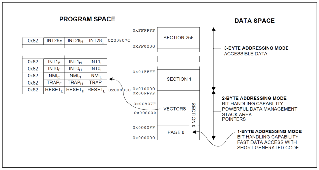
Program Space
The Program Space is where the instructions and their immediate data are stored. Since this is a logical space, it has the same 16 MiB address space. It starts at 0x000000 and ends at 0xFFFFFF. We use hexadecimal format for specifying memory addresses since the values can be very long when represented in decimal format.
The Program Space is logically partitioned to Pages and Sections for the efficient handling of memory accessing. A Page is a 256-bytes long contiguous memory section. The address range of a Page can be from 0xXXXX00 to 0xXXXXFF, where the XXXX is the page number and remains the same for all locations on the same page.
A Section is a 64-kilobytes long contiguous memory section. Since Pages are smaller than Sections, a Section consists of multiple Pages, precisely 256 Pages. The address range of a Section is from 0xXX0000 to 0xXXFFFF, where the XX indicates the Section number. But why is there is such a distinction? You will understand it when we start to explain the assembly programs.
Since the Program Space hold the program, we must also talk about the Interrupt Vectors. It is a list of memory addresses stored in the memory itself. There are 32 entries in the STM8S vector table and they are stored at address starting from 0x8000. Each entry is 32-bit long, stored as 4 bytes. The most significant byte of all of these entries is a reserved op-code of 0x82. Followed by that are three variables bytes E (Extended), H and L as shown in the previous diagram.
As you can see, the vector table starts at 0x008000 and ends at 0x00807C. The first three entries of the vector table are RESET, Trap and NMI (Non-Maskable Interrupt). The remaining 29 user interrupt vectors. The RESET vector is placed at 0x8000 and the microcontroller starts executing the instruction pointed by the memory address stored at this vector. The Flash memory of the STM8 microcontroller is part of the Program Space.
Data Space
The Data Space is where the temporary data is stored when the microcontroller is working. It is the working memory of the computer and is also where the RAM resides. As you can see from the previous diagram, there are different sections of the memory that supports different types of addressing modes. The Page 0, for example, supports 1-byte addressing and has bit addressing capability. That means, we can change the state of single bits at these locations.
Similarly, the entire Section 0 has 2-byte addressing capability and bit handling feature. Sections from 1 to the remaining 256 only support 3-byte addressing modes and without bit handling. This will become more obvious once we start using the STM8 instruction set.
Memory Map
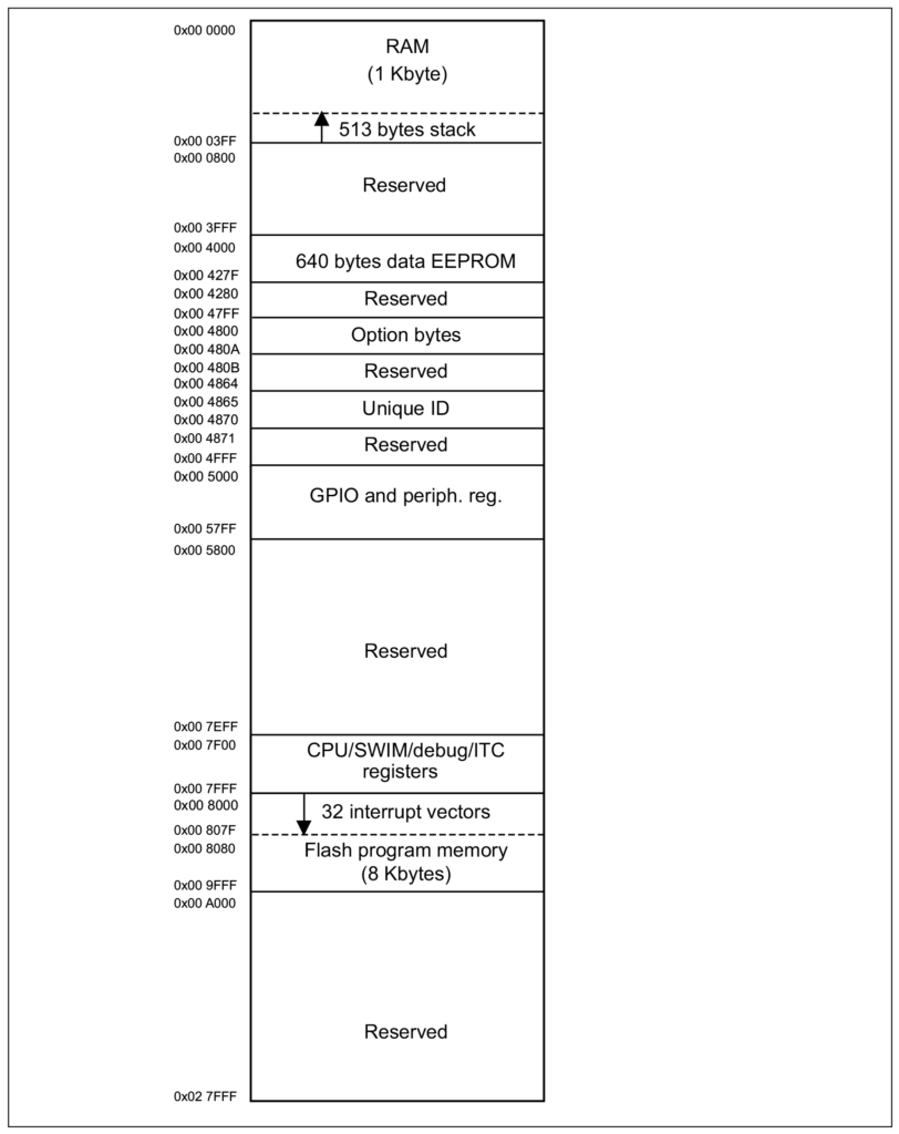
We know that the Memory Space of the STM8S series processor is 16 MiB wide and it is not practically as large as that. The Memory Map tells us where the actual usable memory locations are. This is better understood by the memory map diagram found on the STM8S103F3P6 datasheet. All areas marked as “Reserved” are inaccessible. Everything else is self-explanatory at this point.
Led Blink Program
Enough talking. Time to write some program. Our first Assembly program is going to blink the TEST LED connected to the GPIO pin PB5. To follow this section, you need all of the hardware we asked you to get in the previous tutorial and all of the software tools should be installed properly.
Creating A Project
Let’s start by creating a project first. First we suggest creating a common folder for all of your STM8 programs. We will then create sub-folders for each of the project. Create a project directory called Blink and create a new file called main.asm in there. You can open the project folder in VS Code and add it. Use the Copy button on the top-right corner to copy the code and then paste it into the file.
.stm8
;
; STM8 assembler LED blink demo
; Version 0.2

F_CPU         EQU   16000000  ; CPU clock frequency, required by delay routines
LED           EQU   5  ; LED pin index on Port B
DELAY         EQU   100  ; Blink interval in ms

CLK_CKDIVR    EQU   0x50C6 ; Clock divider register
PB_DDR        EQU   0x5007 ; Port B data direction register
PB_CR1        EQU   0x5008 ; Port B control register 1
PB_CR2        EQU   0x5009 ; Port B control register 2
PB_ODR        EQU   0x5005 ; Port B data output latch register

; CLK_CKDIVR flags
HSIDIV_00     EQU   0x00  ; HSI prescaler: fHSI / 1
CPUDIV_000    EQU   0x00 ; CPU prescaler: fMASTER / 1

; Code starts at this address
.org 0x8080

start:
    MOV     CLK_CKDIVR, #(HSIDIV_00 | CPUDIV_000)  ; clock setup
    BSET    PB_DDR, #LED  ; set the LED pin as output
    BSET    PB_CR1, #LED  ; set the LED pin as push-pull
    BSET    PB_CR2, #LED  ; set the output speed to high (<= 10MHz)

loop:
    LDW     X, #DELAY  ; load the blink interval
    CALL    delay_ms  ; wait for the DELAY ms
    BCPL    PB_ODR, #LED  ; toggle the LED pin
    JP      loop  ; loop forever

.func delay_ms
loop_ms:
    LDW     Y, #((F_CPU / 1000) / 3)    ; set the inner loop to the equivalent of 1000us

loop_cycles:
    DECW    Y                           ; decrement the inner loop
    JRNE    loop_cycles                 ; loop until Y is zero
    DECW    X                           ; decrement the number of milliseconds
    JRNE    loop_ms                     ; loop until X is zero
    RET
.endf

; interrupt vectors
.org 0x8000
    INT     start  ; RESET handler, jump to the main program body
We are calling our program file main because it contains our main logic. But you can name it just anything. The extension .asm indicates an Assembly language file. VS Code will try to use Assembly language-specific styling for the code once it detects the file extension. This example program is adopted from the STM8 Assembler Playground examples.
Assembling
An Assembly language program needs to be “assembled” before we can upload it to the microcontroller. The software tool that does this is called an assembler. We are going to use the NakenASM assembler developed by Michael Kohn. The assembler reads all of the mnemonics, data and other directives and generate a list of op-codes. The assembled file can be saved in different formats, but the Intel HEX format is the most popular. It is simply called a hex file in generic terminology. To assemble our main.asm program, open the Terminal in VS Code and run the following command. You can also run a standalone Terminal window from the folder.
naken_asm main.asm -o main.hex -type hex -lThis will convert the assembly program to an Intel HEX file and write it to main.hex file. Let’s now understand the different parts of the command.
naken_asm– this is how we invoke the NakenASM assembler from the Terminal. Everything following this command will be parameters for the assembler.main.asm– this is how we specify the source file to assemble. Since we are running the Terminal from the same folder, we only need to specify the file name.-o– this is an option to specify the output file. We can add the output file name after this option.main.hex– this is the output file.-type– this is an option to specify what kind of file we want to create.hex– this is the type of file we want to create and it stands for the Intel HEX file.-l– this is an option to ask the assembler to create a list file.
When you run the command, you will get an output similar to what is shown below.
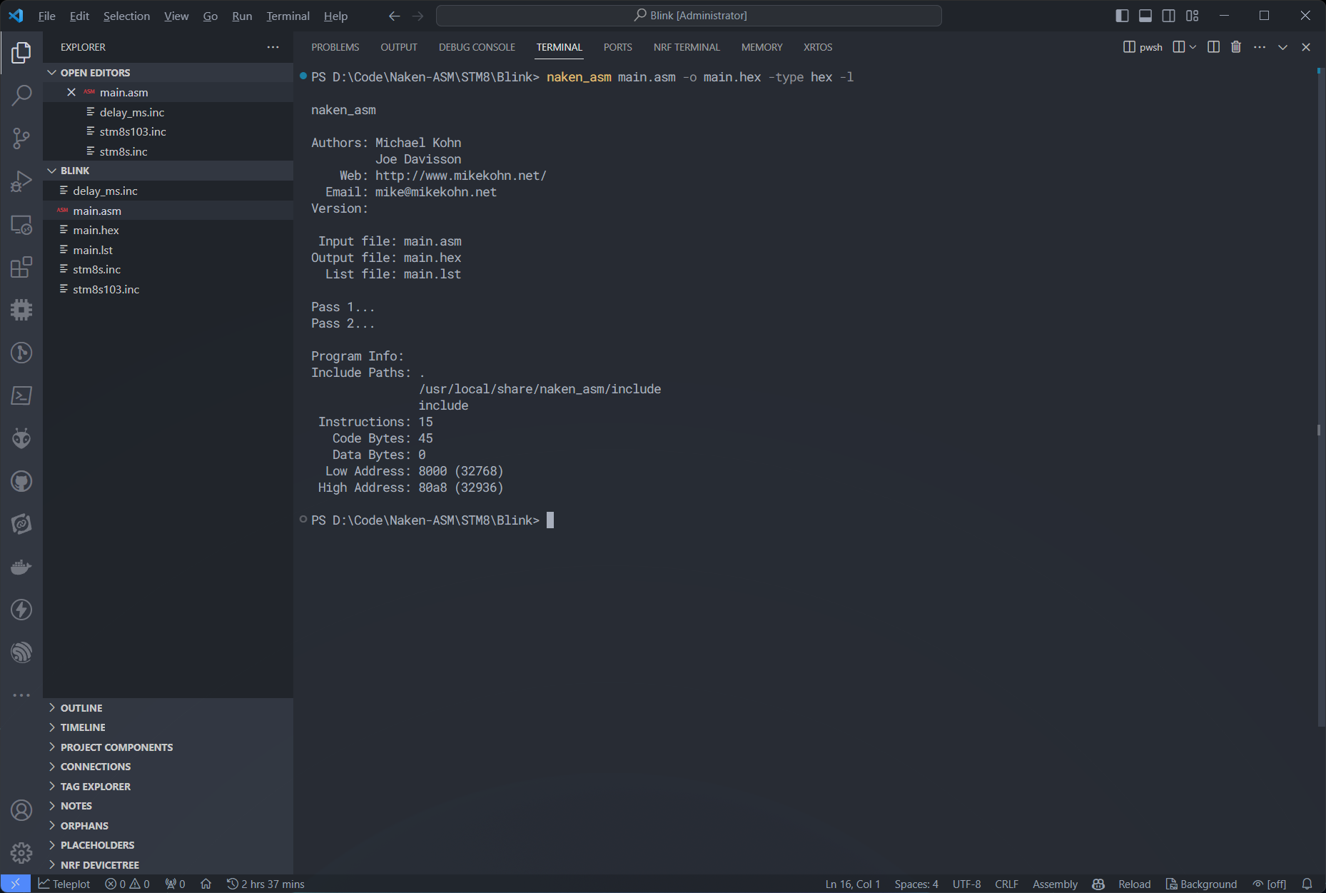
PS D:\Code\Naken-ASM\STM8\Blink> naken_asm main.asm -o main.hex -type hex -l

naken_asm

Authors: Michael Kohn
         Joe Davisson
    Web: http://www.mikekohn.net/
  Email: mike@mikekohn.net
Version:

 Input file: main.asm
Output file: main.hex
  List file: main.lst

Pass 1...
Pass 2...

Program Info:
Include Paths: .
               /usr/local/share/naken_asm/include
               include
 Instructions: 15
   Code Bytes: 45
   Data Bytes: 0
  Low Address: 8000 (32768)
High Address: 80a8 (32936)Let’s see what the output mean. The following lines just print the application information. Interestingly, the version of the application is missing here for some reason. Not an issue for us.
naken_asm

Authors: Michael Kohn
         Joe Davisson
    Web: http://www.mikekohn.net/
  Email: mike@mikekohn.net
Version: The next three lines print the input and output files.
 Input file: main.asm
Output file: main.hex
List file: main.lstThe following lines show how many times the assembler goes through the entire program to find all of the references and apply any optimizations if needed.
Pass 1...
Pass 2...The following lines tell us a few information about the assembling process. The Include Paths are extra folders or files containing any code that is part of the main program. And yes, we can include external files to our main program which we will see later how you can do it.
Program Info:
Include Paths: .
               /usr/local/share/naken_asm/include
               include
 Instructions: 15
   Code Bytes: 45
   Data Bytes: 0
  Low Address: 8000 (32768)
High Address: 80a8 (32936)There are 15 instructions in our assembled code. If you check our main program and count the instructions, it will be 15. So no surprise! There are 45 code bytes which indicates the number of total bytes in our program, including the instruction op-codes. Since we do not have anything to be stored in the EEPROM section, the data bytes count is 0. The Low Address indicates where the start of the program is located and the High Address indicates where the program ends. But 0x80A8 – 0x8000 is 168 bytes. Does that mean our program is 168 bytes long when converted to machine code? No. We know that the address 0x8000 is the RESET vector and it only hold the address of the start program. So where does our program start in the memory? That is what the List file is for. The list file contain the snapshot of the memory of the microcontroller and shows what goes where. But before that let’s check the main.hex file.
Intel HEX File
An Intel HEX is a file format developed by Intel. It stores computer firmware (machine code) represented in hexadecimal text strings in a normal text file. It stores any data in the form of records. A record is made up of 5 fields as shown below.
:llaaaatt[dd...]cc:– the colon indicates the start of the record.ll– this is the record-length field that represents the number of data bytes (dd) in the record.aaaa– the address field that represents the starting address for subsequent data in the record.tt– field that represents the HEX record type, which may be one of the following:00– data record01– end-of-file record02– extended segment address record04– extended linear address record05– start linear address record
dd– data field that represents one byte of data in hexadecimal representation. A record may have multiple data bytes. The number of data bytes in the record must match the number specified by thellfield.cc– the checksum field that represents the checksum of the record. The checksum is calculated by summing the values of all hexadecimal digit pairs in the record through the modulo 256 method and taking the two’s complement.
Now we can explain the hex file of our Blink program. Since the syntax highlighting we use does not support Intel HEX, we will show the screenshot from VS Code.
:0480000082008080FA
:10808000350050C6721A5007721A5008721A5009F9
:10809000AE01F4CD809D901A5005CC809090AE1426
:0980A000D5905A26FC5A26F58100
:00000001FF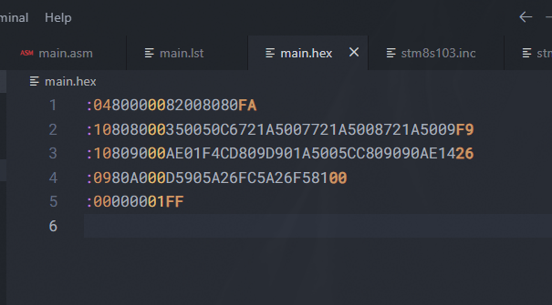
The first byte tells that the first record has 4 data bytes in it and if you count it you would be right. The next two bytes 0x8000 indicates where the record should be saved, which is the location of the RESET vector. The next 0x00 indicates that it is a data record. If you now look at the data bytes, it goes exactly how we expected it to be. The reserved op-code 0x82 appears first followed by the three byte value 0x008080, which is the value of the RESET vector. So when the MCU is reset, the Program Counter loads whatever instruction found at the location 0x8080. The 0xFA at the end is the checksum which an upload tool can use to verify the integrity of the Intel HEX file.
The next record contains 16 bytes (0x10) and starts at 0x8080. This is where the main program starts. The remaining records are also part of our main program. The last record is an EOF record that indicates the end of the file.
List File
Looking at the hex file is not at all obvious when you want to check the machine code of the program. That’s why we have a list file. It combines the original program and the corresponding op-codes generated in a single text file.
.stm8
;
; STM8 assembler LED blink demo
; Version 0.2

F_CPU         EQU   16000000  ; CPU clock frequency, required by delay routines
LED           EQU   5  ; LED pin index on Port B
DELAY         EQU   500  ; Blink interval in ms

CLK_CKDIVR    EQU   0x50C6 ; Clock divider register
PB_DDR        EQU   0x5007 ; Port B data direction register
PB_CR1        EQU   0x5008 ; Port B control register 1
PB_CR2        EQU   0x5009 ; Port B control register 2
PB_ODR        EQU   0x5005 ; Port B data output latch register

; CLK_CKDIVR flags
HSIDIV_00     EQU   0x00  ; HSI prescaler: fHSI / 1
CPUDIV_000    EQU   0x00 ; CPU prescaler: fMASTER / 1

; Code starts at this address
.org 0x8080

start:
    MOV     CLK_CKDIVR, #(HSIDIV_00 | CPUDIV_000)  ; clock setup

0x8080: 35 00 50 c6     mov $50c6, #$00                          cycles: 1

    BSET    PB_DDR, #LED  ; set the LED pin as output

0x8084: 72 1a 50 07     bset $5007, #5                           cycles: 1

    BSET    PB_CR1, #LED  ; set the LED pin as push-pull

0x8088: 72 1a 50 08     bset $5008, #5                           cycles: 1

    BSET    PB_CR2, #LED  ; set the output speed to high (<= 10MHz)

0x808c: 72 1a 50 09     bset $5009, #5                           cycles: 1


loop:
    LDW     X, #DELAY  ; load the blink interval

0x8090: ae 01 f4        ldw X, #$1f4                             cycles: 2

    CALL    delay_ms  ; wait for the DELAY ms

0x8093: cd 80 9d        call $809d                               cycles: 4

    BCPL    PB_ODR, #LED  ; toggle the LED pin

0x8096: 90 1a 50 05     bcpl $5005, #5                           cycles: 1

    JP      loop  ; loop forever

0x809a: cc 80 90        jp $8090                                 cycles: 1


.func delay_ms
loop_ms:
    LDW     Y, #((F_CPU / 1000) / 3)    ; set the inner loop to the equivalent of 1000us

0x809d: 90 ae 14 d5     ldw Y, #$14d5                            cycles: 2


loop_cycles:
    DECW    Y                           ; decrement the inner loop

0x80a1: 90 5a           decw Y                                   cycles: 1

    JRNE    loop_cycles                 ; loop until Y is zero

0x80a3: 26 fc           jrne $80a1  (offset=-4)                  cycles: 1-2

    DECW    X                           ; decrement the number of milliseconds

0x80a5: 5a              decw X                                   cycles: 1

    JRNE    loop_ms                     ; loop until X is zero

0x80a6: 26 f5           jrne $809d  (offset=-11)                 cycles: 1-2

    RET

0x80a8: 81              ret                                      cycles: 4

.endf

; interrupt vectors
.org 0x8000
    INT     start  ; RESET handler, jump to the main program body

0x8000: 82 00 80 80     int $8080                                cycles: 2

data sections:


Program Info:
                         LABEL ADDRESS  SCOPE
                         start 00008080 0
                          loop 00008090 0
                      delay_ms 0000809d 0
                       loop_ms 0000809d 1
                   loop_cycles 000080a1 1
 -> Total symbols: 5

Include Paths: .
               /usr/local/share/naken_asm/include
               include
 Instructions: 15
   Code Bytes: 45
   Data Bytes: 0
  Low Address: 0x8000 (32768)
 High Address: 0x80a8 (32936)
For example, on line 24 we can see the actual line of code and on line 26, the op-codes generated. The cycles indicate the number of clock cycles it takes to the execute that instruction. We will explain every line of the code later down below. You will then be able to look at the list file again and figure out what is going on. Before that, let’s upload our Blink program to the Flash memory of the STM8 microcontroller. The assembled form of program is usually called a firmware.
Uploading
We can use either the STM8Flash tool or the official STVP tool to upload the firmware. You need to connect the ST-Link V2 debugger to the board and connect both the debugger and the STM8S-Blue board to the computer.
| STM8S-Blue | STLink-V2 |
|---|---|
NRST | RST |
SWIM | SWIM |
GND | GND |
STM8Flash
Open a Terminal in the project folder where the hex file is, and run the command shown below.
stm8flash -c stlinkv2 -p stm8s003f3 -w main.hexIf successful, it will print the number of bytes written to the microcontroller and the TEST LED will start blinking.
PowerShell 7.4.2
PS D:\Code\Naken-ASM\STM8\Blink> stm8flash -c stlinkv2 -p stm8s003f3 -w main.hex
Determine FLASH area
libusb: error [init_device] device '\\.\USB#VID_1532&PID_0099&MI_03#6&3475DE72&0&0003' is no longer connected!
libusb: warning [force_hcd_device_descriptor] could not infer VID/PID of HCD hub from '\\.\ROOT#USB#0000#{3ABF6F2D-71C4-462A-8A92-1E6861E6AF27}'
libusb: warning [force_hcd_device_descriptor] could not infer VID/PID of HCD hub from '\\.\ROOT#USB#0000#{3ABF6F2D-71C4-462A-8A92-1E6861E6AF27}#UDE'
libusb: error [init_device] device '\\.\USB#VID_046D&PID_0825&MI_02#8&1DF2C811&0&0002' is no longer connected!
Due to its file extension (or lack thereof), "main.hex" is considered as INTEL HEX format!
169 bytes at 0x8000... OK
Bytes written: 169
PS D:\Code\Naken-ASM\STM8\Blink>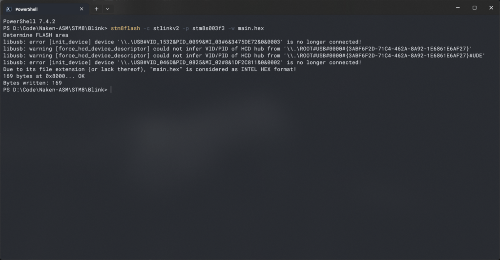
You can see that there are a few errors printed by the tool which are related to the debugger ID. Regardless of that, the uploading operation is successful. The format of invoking the STM8Flash tool is as shown below.
stm8flash -c <stlink|stlinkv2|espstlink> -p <partname> [-s flash|eeprom|0x8000] [-r|-w|-v] <filename>STVP
ST Visual Programmer (STVP) is a GUI tool from STMicroelectronics to program and read STM8 microcontrollers using ST-Link programmer/debugger tool. Connect the ST-LinkV2 debugger the same way we connected before. Connecting the NRST pin is optional for STVP.
Since we have already written the blink program to the STM8 board we can try reading it back. Change the tab to PROGRAM MEMORY and click on Read → Current Tab. This will read the flash contents to the current display tab.
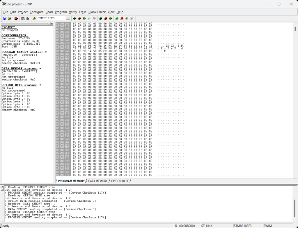
If for some reason, you are not able to read/write to the board, try setting the ROP in OPTION BYTE tab to Read Out Protection OFF. Then write the Option Bytes using the Program → Current Tab option. You might have to do this for the first time when you try to use the board.
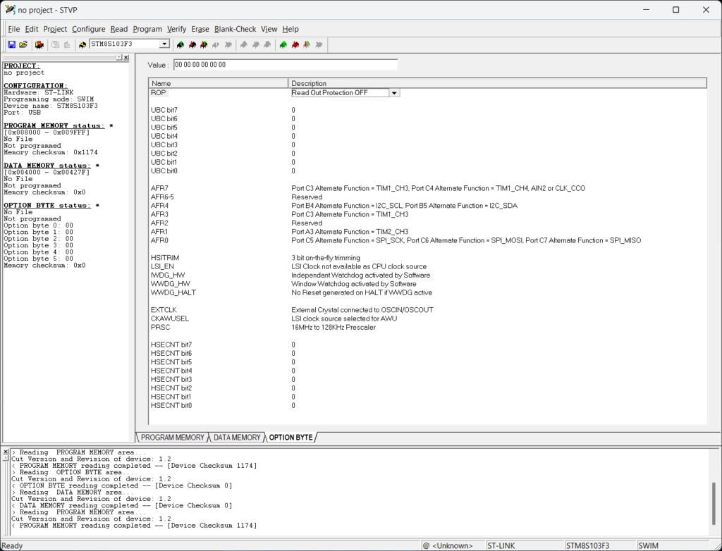
You can also program the STM8 board using the hex file we just created. Open the PROGRAM MEMORY tab, right click inside and click Open to open the hex file. This will load the hex file to the tab. You can check the memory checksum to verify that the program we loaded from file and that read from the chip are the same. In this case, the checksum is 0x1174.
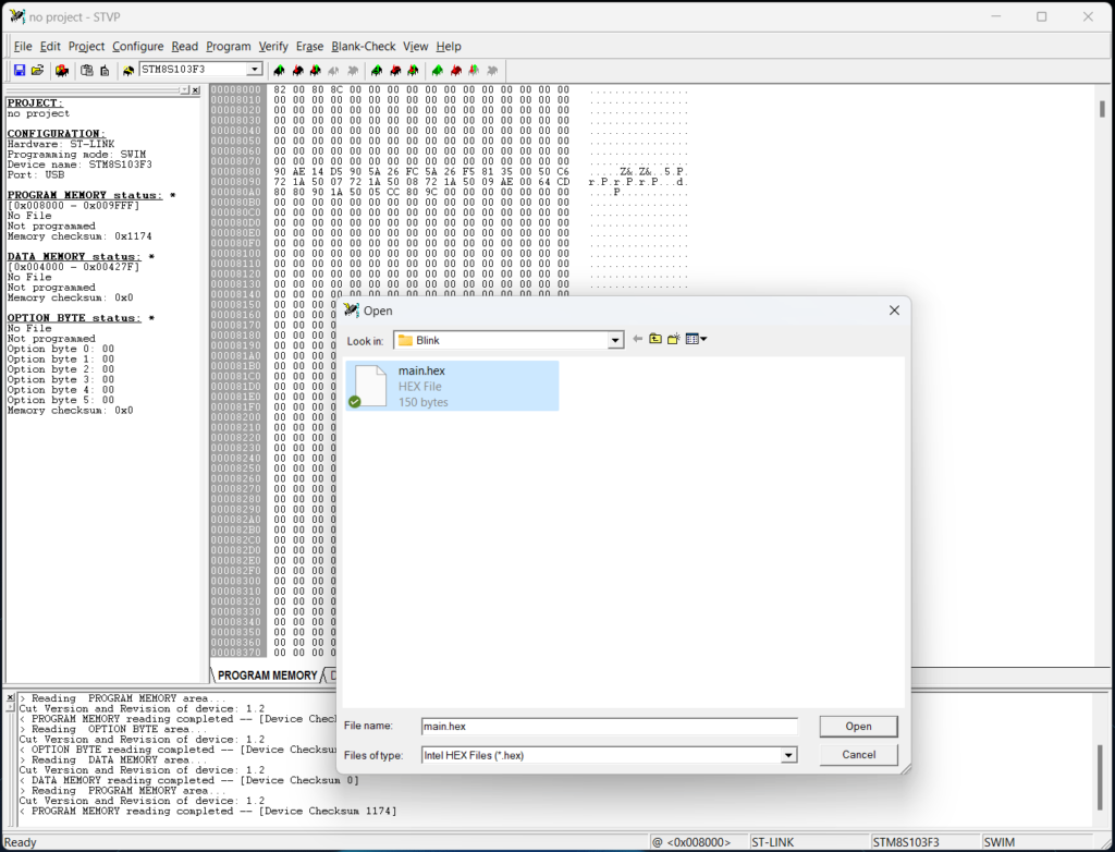
Use Program → Current Tab to write the firmware to the STM8 chip. The code will not run immediately on the board if the NRST pin is connected. This is because, the NRST pin will be pulled-low by the ST-Link V2 programmer after an operation. Simply close the application or disconnect the NRST wire to run the program on the board. The STM8Flash application will not work when the STVP application is running as it binds to the debugger hardware.
Code Explanation
We can now begin to explain the code.
.stm8The first line starting with .stm is an Assembler Directive. Anything that starts with a . is one. An assembler directive an instruction to the assembler itself. It is not an instruction or data for our program logic. In this case, .stm8 means, the assembly program is meant for the STM8 platform supported by NakenASM. There are many other platforms supported and the directive at the start of the program tells which assembler to use.
; STM8 assembler LED blink demoThis is a comment. Anything that starts with a ; character is a comment. Comments can take entire lines or appear at the end of a program statement.
F_CPU         EQU   16000000  ; CPU clock frequency, required by delay routines
LED           EQU   5  ; LED pin index on Port B
DELAY         EQU   100  ; Blink interval in ms

CLK_CKDIVR    EQU   0x50C6 ; Clock divider register
PB_DDR        EQU   0x5007 ; Port B data direction register
PB_CR1        EQU   0x5008 ; Port B control register 1
PB_CR2        EQU   0x5009 ; Port B control register 2
PB_ODR        EQU   0x5005 ; Port B data output latch register

; CLK_CKDIVR flags
HSIDIV_00     EQU   0x00  ; HSI prescaler: fHSI / 1
CPUDIV_000 EQU 0x00 ; CPU prescaler: fMASTER / 1All of these are reusable constants that we can use anywhere in the program. The EQU is also an assembler directive. It tells the assembler to treat the value of a constant the same everywhere in the program. For example, where LED appears, the value has to be considered to be 5. Why is this important? It allows us to define the value of a constant in a single place and reuse it any number of times. If we ever wanted to change the LED pin to another value, say 6, we can change that in the line 7 only and the effect will appear everywhere in the program. The usage is similar to the #define macro (defined constants) in a C/C++ program.
The directive EQU means “equal” and it is not case-sensitive; “EQU” and “equ” means the same thing. But the constant names are case-sensitive; “LED” is not equal to “led“. The format of EQU directive is,
<constant name> EQU <constant value>The next line is also an assembler directive. It sets the origin address of the remaining code to come just after the directive. In this case, the MOV instruction on line 24 will be stored at 0x8080.
.org 0x8080This should be obvious to you now. Because we know from the memory map of STM8S103F3P6 that the Flash memory starts at 0x8080. This is start of the 8 KiB flash memory section where we can store our programs. It starts at 0x8080 and ends at 0x9FFF.
The following line creates a label called start. Labels are a way of specifying relative memory locations that we can reuse at other parts of the program. When the program is assembled, the label takes up the value of an actual memory address and we can direct the flow of the program to that location using jump instructions. You just need to suffix a word with : character to create a label. We will use the start label later to set the reset interrupt vector. Labels are case-sensitive.
start:MOV
Next is our first STM8 instruction. MOV is part of a set of instructions called Load and Transfer. MOV literally means “move”. It moves data from one memory location to another.
MOV CLK_CKDIVR, #(HSIDIV_00 | CPUDIV_000) ; clock setupThe format of the MOV instruction is:
MOV <destination>, <source>The MOV instruction moves the value at source address to the destination address. The source and destination can be specified in a few different ways, determined by the addressing modes. Following are the addressing modes supported by MOV.
- An immediate byte to a direct memory location.
- A direct memory location to another direct memory location (from
$00to$FF). - A direct memory location to another direct memory location (from
$0000to$FFFF).
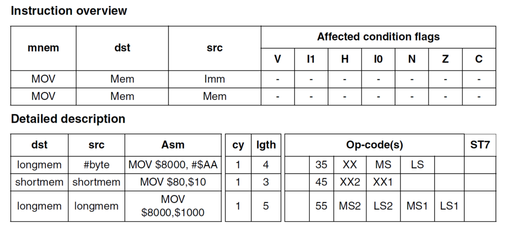
As you can see from the table above, the advantage of using different addressing modes is that we can reduce the size of the instructions and therefore save memory space and make the program faster. The Accumulator (A) register is not affected when a data is moved, nor the Condition Code flags (CC register).
If we revisit the original line of code, we are moving a byte value to a memory location pointed by CLK_CKDIVR which is equal to 0x50C6. So we are using the first addressing mode.
MOV CLK_CKDIVR, #(HSIDIV_00 | CPUDIV_000) ; clock setupWe are using an immediate value for the source here. An immediate value in an assembly program is prefixed with # character. For example #5. We can specify numbers in decimal or hexadecimal formats. Hex values should be prefixed with $ symbol. For example, $5. We can also have expressions for an immediate value. In our case, the expression is (HSIDIV_00 | CPUDIV_000) and it OR operates the two constant values we have defined earlier. This logical OR operation is done by the assembler, not the processor. So an assembler can also do calculations and logic operations for us. This saves us from doing manual calculations, which is nice.
When you OR operate HSIDIV_00 (0x00) and CPUDIV_000 (0x00), you get 0x00; no surprise. So the effective instruction line becomes,
MOV 0x50C6, #$00 ; clock setupIf you now check the datasheet of STM8 and see what resides at the address 0x50C6, we can see that it is part of the clock-specific register set and the 0x50C6 is a single byte that sets the clock divider value.
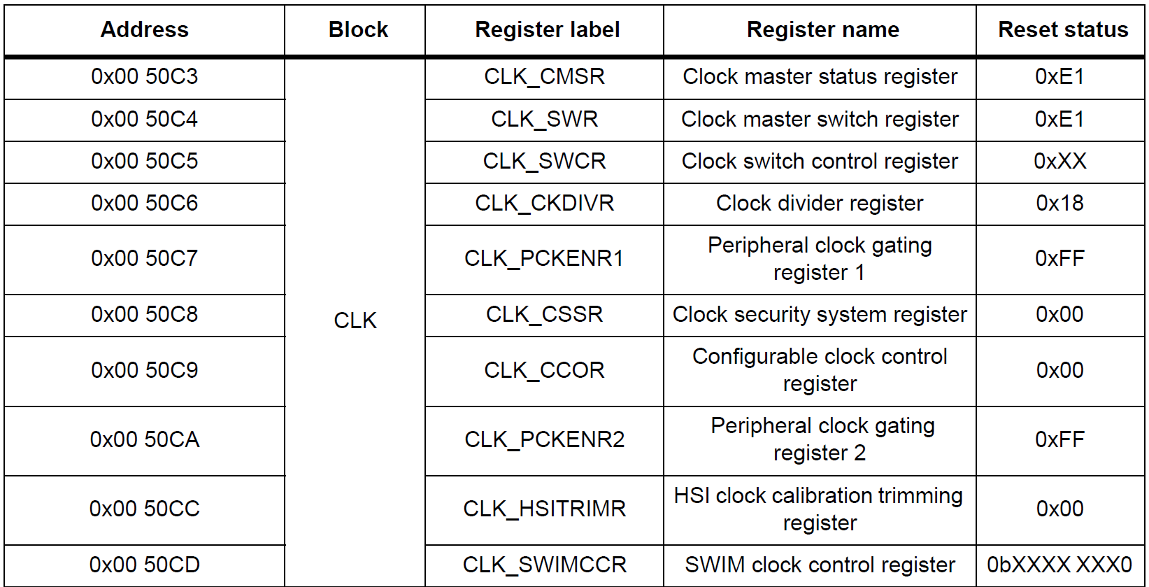
The definition of the register is as follows. It sets the prescalars for both the HSI (High Speed Internal) clock and the CPU clock input. As we are setting both values to 0, we keep the clock frequency to the maximum, which is 16 MHz.
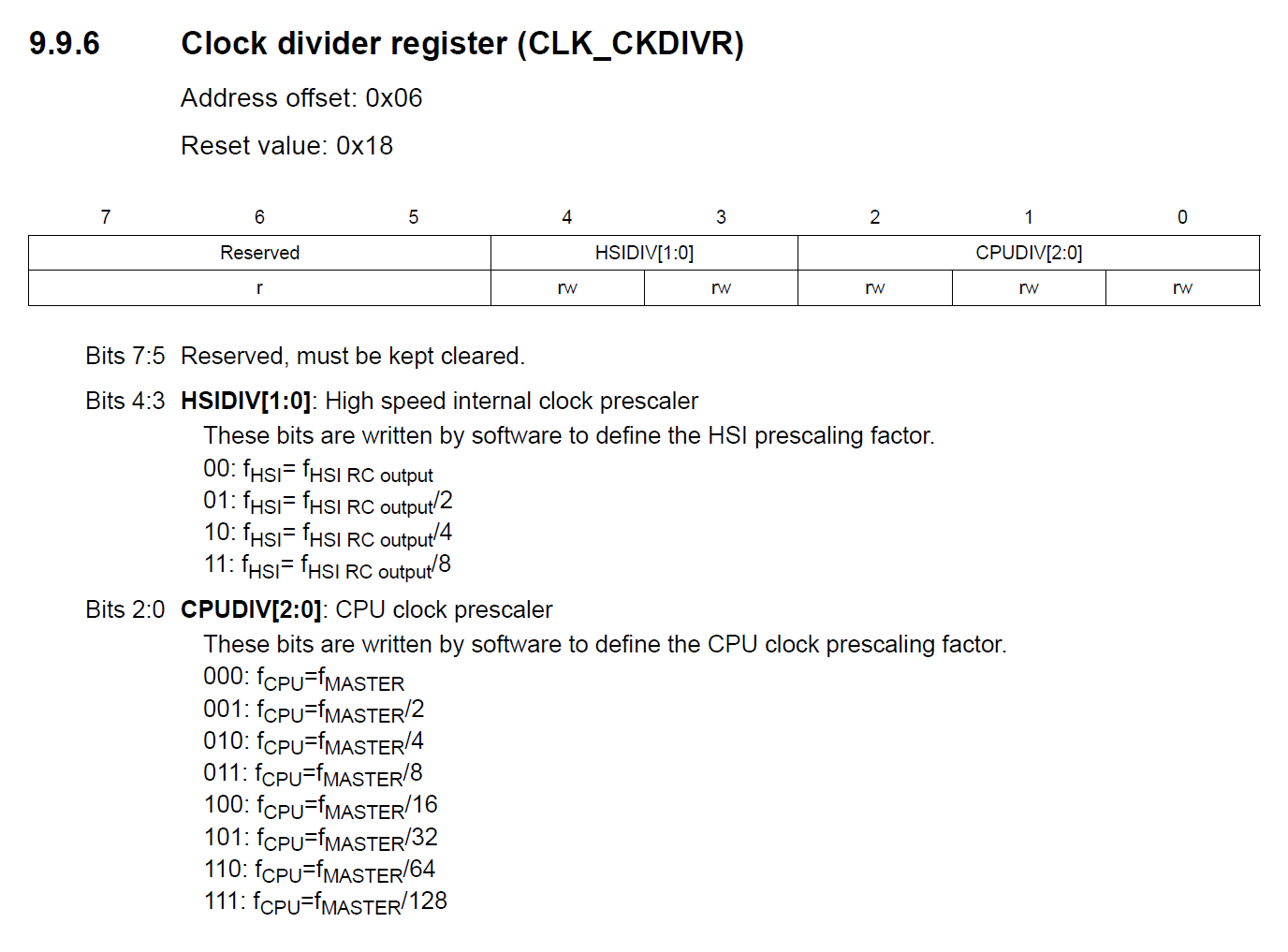
Setting the clock is an important thing we have to do before we begin the main logic of our program.
BSET
BSET  PB_DDR, #LED  ; set the LED pin as output
BSET  PB_CR1, #LED  ; set the LED pin as push-pull
BSET PB_CR2, #LED ; set the output speed to high (<= 10MHz)We have a new instruction here. BSET (Bit Set) is an instruction to set a single bit at the specified memory location. The instruction is a combination of three operations.
- Read the destination byte.
- Change the specified bit to
1. - Write the resulting value back to the destination.
The BSET is very fast and is useful for bit manipulations. There is only one addressing mode for this instruction.

The TEST LED on the STM8S-Blue board is connected to the PB5 pin of the microcontroller. To control an LED, we need to
- Set the pin to an output type.
- Set the the type of output (push-pull or open-drain)
- Set pin speed (2 MHz or 10 MHz)

So with the three BSET instructions, we are setting the PB5 pin to a push-pull output with 10 MHz speed. Notice how we used the same #LED constant value of 5 with all the three instructions. If we ever want to change the pin, we can do that easily by changing the definition of the LED constant.
Next we have another label called loop. We will use this memory location as a jump destination to do a task repeatedly.
loop:LDW
The loop is to create a delay. During the delay time, the CPU will “waste” its time until the delay is exhausted. This delays the next operation in line. We start with a new instruction called LDW which stands for Load Word. A word in computing is 16-bit. So the LDW instruction will load a 16-bit value (2 bytes) to a 16-bit destination. This instruction must use X, Y, or SP as one of its operands.
This instruction has many variations and so we won’t be discussing all of them here. Just remember that the LDW instruction covers enough variations to support most of the use-cases. Following is the type of addressing we are using here.

The following line moves the DELAY value of decimal 100 to the X register. The assembler takes care of converting the value 100 to a 16-bit value.
LDW X, #DELAY ; load the blink intervalCALL
CALL is an instruction to call a function/subroutine. A function is a group of instructions that are logically bound and usually accomplishes a single task. When a task needs to be performed multiple times in different parts of a program, we can group the instructions required for the task as a function. Here, the function we are calling is the delay_ms which generates a delay in multiple of a millisecond. We need this to wait before we can toggle the LED.
When CALL is invoked, the lower two bytes of the the PC (H and L) are pushed to the stack in SRAM and the destination address of the function is loaded. Since the E byte of PC is not stacked into the SRAM, the function being called must be within the same 16-bit memory section. CALL must be preceded with a RET instruction to load the saved PC contents from the stack back to the PC.
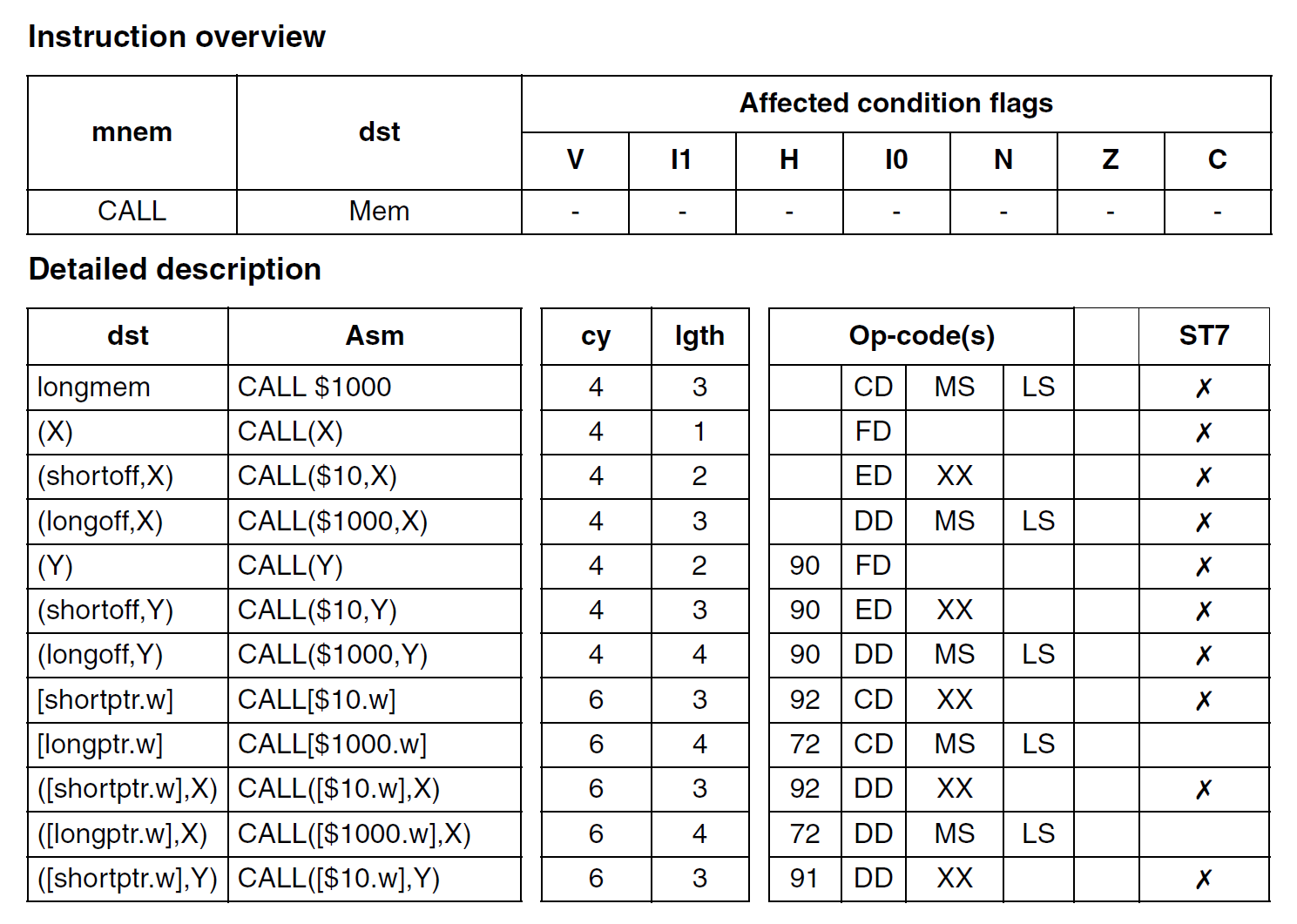
CALL delay_ms ; wait for the DELAY msWhen we call the delay function, the address of the first instruction of the delay_ms function is loaded into the PC. After the delay_ms function is complete, the control is returned back to the calling section. The code then resumes from the instruction just after the CALL instruction. We will see how the function returns the control back to the calling function.
BCPL
BCPL PB_ODR, #LED ; toggle the LED pinBCPL is a bit manipulation instruction that complements the bit field of a byte at the destination memory. All other bits remain unchanged. Here, we are using the BCPL instruction to toggle the output state of the output data latch register associated with GPIO 5 of Port B (PB_ODR, 0x5007). When the instruction is repeatedly called with a delay in between, it will blink the LED.
JP
JP loop ; loop foreverThe JP instruction jumps to the specified destination. The type of jump operation is called an absolute or unconditional jump since it doesn’t check for any satisfaction of conditions. The operation replaces the content of Program Counter with the specified address. CC register is not affected.
Here, the location is indicated by a label called loop. When the JP instruction is invoked, whatever the address of loop is, the PC will load that and execute the instructions from there.
The following line is an assembler directive that indicates the start of a function. A function is also called a routine. .func followed by a unique function name is how we define a function. The assembler will know that we are defining a function, and will replace the function name with the address of the function whenever it is called with a CALL instruction.
The function name is case-sensitive and it should be unique. Whitespaces are not allowed in function names. Use underscores (_) instead. Here, the delay_ms function creates a delay before we can toggle the LED state.
.func delay_msThe next line is a label called loop_ms. This is the start of the function, but not a location in memory.
loop_ms:The next line the first instruction inside the function. It is again an LDW instruction. But this time, we are using the index register Y as the destination. With the equation on the source side, we are asking the assembler to do some math for us. It calculates a decimal value of steps needed to create a delay in terms of clock cycles. If we know the period of a single clock cycle, we can create any delay as a multiple of that time period. That is essentially we are doing here. Here, the delay we need is 1 ms.
LDW Y, #((F_CPU / 1000) / 3) ; set the inner loop to the equivalent of 1000usThe effective value of X will become,
LDW Y, #$14D5 ; set the inner loop to the equivalent of 1000usBut how does the calculation work? The CPU runs at a 16 MHz clock. So the period of a clock cycle is,
Cycle Period = 1 / (16 x 106) = 62.5 ns (62.5 x 10⁹)
If a single cycle period is 62.5 nanosecond, as we will see in a moment, we need to execute two instructions in a loop to produce that delay. The first instruction LDW takes 1 cycle and the second instruction JRNE takes 2 cycles. That means, it will take 3 cycles to execute the two instructions.
Total time = 3 * 62.5 ns = 187.5 ns
We need to create a delay of 1 m or 1000 us. So it will take,
Total loops = 1000000 ns / 187.5 ns = 5333.33 ≈ 5333
So we need to execute the loop around 5333 times to produce a delay of 1 ms. The decimal value 5333 can be converted to hex as 0x14D5. The same calculation is done at line 37 by the assembler. As we will see further, we will call this section of the code repeatedly to produce longer delays.
In the next line, we create another label called loop_cycles. This is the loop that creates the delay for the total time.
loop_cycles:DECW
The next line is a new instruction. DECW is used to decrement a single word (16-bit value). Decrementing is simply subtracting 1 from the existing value. Here, we are decrementing the value of the index register Y.
DECW Y ; decrement the inner loop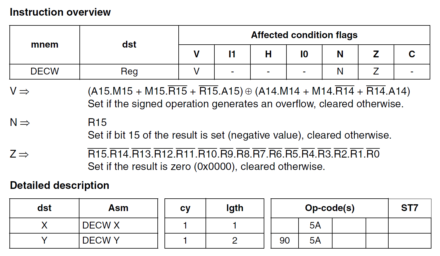
Since subtracting is an arithmetic operation, some of the CC register flags are affected. We can use the state of these flags to make jump decisions.
JRNE
JRNE stands for “Jump if Not Equal”. Equal to what you ask! The easiest way to determine if two numbers are equal is subtracting one from the other. If they are equal, the result will be 0. So whenever we do a subtraction operation with the processor, if the result is 0, then the Z condition flag is set in the CC register.
So when we decrement the value of the Y register, if it becomes 0 at some point, the Z flag is set. The JRNE instruction checks the state of the Z flag and if is not set, jumps to the specified location. On the other hand, if the Z is set, JRNE skips the operation and the program continues from the next instruction.
JRNE loop_cycles ; loop until Y is zeroIn this case, the program jumps to the loop_cycles label if the value in Y is not 0.
In the next line, we decrement the value in X. If you remember, we had loaded X with the value in milliseconds of delay we want between toggling the LED. The value was 100. So every time we call this instruction, the value is decremented from 100, repeatedly, until it becomes 0.
DECW X ; decrement the number of millisecondsThe next line causes the program to jump to the loop_ms label if the resultant value after decrementing X is still not 0.
JRNE loop_ms ; loop until X is zeroRET
RET is the instruction to return from a normal function. It loads the PC with the saved contents from stack. This takes the program control back to where the call was originated from.
RETThe next line is an assembler directive that marks the end of a function.
.endfLet’s now take a look at the entire function as a whole. Before calling this function, we must load the register X with the delay value in milliseconds. There are two loops here; one for creating the delay of a single millisecond and another one for repeating the millisecond delay for a number of times.
With the explanation we had so far, you will be able to read and understand how this function as a whole works.
.func delay_ms
loop_ms:
    LDW     Y, #((F_CPU / 1000) / 3)    ; set the inner loop to the equivalent of 1000us

loop_cycles:
    DECW    Y                           ; decrement the inner loop
    JRNE    loop_cycles                 ; loop until Y is zero
    DECW    X                           ; decrement the number of milliseconds
    JRNE    loop_ms                     ; loop until X is zero
    RET
.endfINT
We just have two lines remaining in the program. We first start a new origin at address 0x8000. Then use the INT instruction to store the address indicated by the start label to the location 0x8000. As per the interrupt vector table, the first location of the table, 0x8000 holds the reset interrupt vector. In other words, the CPU executes the instruction at the memory location pointed by the 0x8000 address, after it is reset. We want the start label to be the start of our program, and so we save that location to the reset interrupt vector.

Unlike other instructions, the INT instruction does not generate a machine code. Instead, the assembler will store the memory address pointed by the start label.
; interrupt vectors
.org 0x8000
INT start ; RESET handler, jump to the main program bodyMachine Code
Machine Code refers to the actual binary information generated from a program. It is the only format the computer can understand, and conversely very difficult for humans to read. Sometimes it can be helpful to look at the machine code to find an issue with the code. Moreover, if you have the machine code of a program, you can also convert it into its equivalent Assembly instructions. This process is called Disassembling. NakenASM also supports disassembling machine code. We can use the NakenUtils application, which is part of the NakenASM, to do that. Since we already have a hex file of our program, we can try disassembling it using the following command.
naken_util -disasm -stm8 main.hexThis will convert the machine codes to a list of addresses, opcodes, instructions, and the number of cycles they consume. This gives us the perfect picture of the memory.
PS D:\Code\Naken-ASM\STM8\Blink> naken_util -disasm -stm8  main.hex

naken_util - by Michael Kohn
                Joe Davisson
    Web: https://www.mikekohn.net/
  Email: mike@mikekohn.net

Version:

Loaded main.hex of type hex / stm8 from 0x8000 to 0x80a8
Type help for a list of commands.

Addr     Opcode         Instruction                              Cycles
-------  ------------   ----------------------------------       ------
0x8000:  82 00 80 80    int $8080                                2
0x8004:  00 00          neg ($00,SP)                             1
0x8006:  00 00          neg ($00,SP)                             1
0x8008:  00 00          neg ($00,SP)                             1
0x800a:  00 00          neg ($00,SP)                             1
0x800c:  00 00          neg ($00,SP)                             1
0x800e:  00 00          neg ($00,SP)                             1
0x8010:  00 00          neg ($00,SP)                             1
0x8012:  00 00          neg ($00,SP)                             1
0x8014:  00 00          neg ($00,SP)                             1
0x8016:  00 00          neg ($00,SP)                             1
0x8018:  00 00          neg ($00,SP)                             1
0x801a:  00 00          neg ($00,SP)                             1
0x801c:  00 00          neg ($00,SP)                             1
0x801e:  00 00          neg ($00,SP)                             1
0x8020:  00 00          neg ($00,SP)                             1
0x8022:  00 00          neg ($00,SP)                             1
0x8024:  00 00          neg ($00,SP)                             1
0x8026:  00 00          neg ($00,SP)                             1
0x8028:  00 00          neg ($00,SP)                             1
0x802a:  00 00          neg ($00,SP)                             1
0x802c:  00 00          neg ($00,SP)                             1
0x802e:  00 00          neg ($00,SP)                             1
0x8030:  00 00          neg ($00,SP)                             1
0x8032:  00 00          neg ($00,SP)                             1
0x8034:  00 00          neg ($00,SP)                             1
0x8036:  00 00          neg ($00,SP)                             1
0x8038:  00 00          neg ($00,SP)                             1
0x803a:  00 00          neg ($00,SP)                             1
0x803c:  00 00          neg ($00,SP)                             1
0x803e:  00 00          neg ($00,SP)                             1
0x8040:  00 00          neg ($00,SP)                             1
0x8042:  00 00          neg ($00,SP)                             1
0x8044:  00 00          neg ($00,SP)                             1
0x8046:  00 00          neg ($00,SP)                             1
0x8048:  00 00          neg ($00,SP)                             1
0x804a:  00 00          neg ($00,SP)                             1
0x804c:  00 00          neg ($00,SP)                             1
0x804e:  00 00          neg ($00,SP)                             1
0x8050:  00 00          neg ($00,SP)                             1
0x8052:  00 00          neg ($00,SP)                             1
0x8054:  00 00          neg ($00,SP)                             1
0x8056:  00 00          neg ($00,SP)                             1
0x8058:  00 00          neg ($00,SP)                             1
0x805a:  00 00          neg ($00,SP)                             1
0x805c:  00 00          neg ($00,SP)                             1
0x805e:  00 00          neg ($00,SP)                             1
0x8060:  00 00          neg ($00,SP)                             1
0x8062:  00 00          neg ($00,SP)                             1
0x8064:  00 00          neg ($00,SP)                             1
0x8066:  00 00          neg ($00,SP)                             1
0x8068:  00 00          neg ($00,SP)                             1
0x806a:  00 00          neg ($00,SP)                             1
0x806c:  00 00          neg ($00,SP)                             1
0x806e:  00 00          neg ($00,SP)                             1
0x8070:  00 00          neg ($00,SP)                             1
0x8072:  00 00          neg ($00,SP)                             1
0x8074:  00 00          neg ($00,SP)                             1
0x8076:  00 00          neg ($00,SP)                             1
0x8078:  00 00          neg ($00,SP)                             1
0x807a:  00 00          neg ($00,SP)                             1
0x807c:  00 00          neg ($00,SP)                             1
0x807e:  00 00          neg ($00,SP)                             1
0x8080:  35 00 50 c6    mov $50c6, #$00                          1
0x8084:  72 1a 50 07    bset $5007, #5                           1
0x8088:  72 1a 50 08    bset $5008, #5                           1
0x808c:  72 1a 50 09    bset $5009, #5                           1
0x8090:  ae 01 f4       ldw X, #$1f4                             2
0x8093:  cd 80 9d       call $809d                               4
0x8096:  90 1a 50 05    bcpl $5005, #5                           1
0x809a:  cc 80 90       jp $8090                                 1
0x809d:  90 ae 14 d5    ldw Y, #$14d5                            2
0x80a1:  90 5a          decw Y                                   1
0x80a3:  26 fc          jrne $80a1  (offset=-4)                  1-2
0x80a5:  5a             decw X                                   1
0x80a6:  26 f5          jrne $809d  (offset=-11)                 1-2
0x80a8:  81             ret                                      4
In order to save the disassembled contents for later, we can direct the output to a file. Run the following command for that.
naken_util -disasm -stm8 main.hex > main.dasmThis will create a new file called main.dasm in the root directory. You can open this file in VS Code to view the assembly instructions. For the syntax highlighting, you can set it to STM8 Disassembly.

What’s Next?
That was quite a journey. We hope we have covered every bits and bytes you want to know to get started with writing Assembly language program for the STM8S family of microcontroller. If you did not understand something, because we did not explain it well, ran into any troubles, please let us know in the comments. This tutorial series is for the absolute beginners. So we do not want to miss anything here.
In the next tutorial, we will learn how to debug the Blink program and see the inside of the microcontroller like a magician. With the super powers of programming and debugging combined, nothing can stop you.
When you are ready, check out the next tutorial in this series. Happy programming 😊
Blinking LED with Timer Interrupts : Learn Microcontroller with STM8S – Tutorial Part #5
Links
- What is A Microcontroller? : Learn Microcontroller with STM8S – Tutorial Part #1 – CIRCUITSTATE Electronics
- NakenASM – Official Website
- NakenASM – GitHub
- STM8 Assembler Playground
- STM8S Series – Official Product Page
- STM8S103F3 Datasheet [PDF]
- AN2752 – Getting Started with STM8S and STM8AF Microcontrollers [PDF]
- PM0044 – STM8 CPU Programming Manual [PDF]
- RM0016 – STM8S and STM8AF Series 8-Bit Microcontrollers [PDF]
- STM8 Product Lineup [PDF]
Short Link
- A short URL to this page – https://www.circuitstate.com/stm8asmprogram
