What is A Microcontroller? : Learn Microcontroller with STM8S – Tutorial Part #1
Learn how a microcontroller works with the help of the STM8S 8-bit microcontroller and learn how to program it with this tutorial series.

We have been sharing microcontroller programming tutorials for some time now. With the rise of affordable and beginner-friendly microcontroller board platforms like Arduino, anyone can build a smart device without needing an engineering degree. But most people who are introduced to the world of microcontrollers in this way tend to skip learning how everything works under the hood. If you are someone who wants to learn how a modern microcontroller actually works inside-every bits and bytes of their operations-you are in the right place. Because this is our first tutorial of a series that tries to teach microcontrollers and their programming from the ground up. We selected the STM8S103F3P6 8-bit microcontroller from the STM8S family produced by ST Microelectronics. You need some basic electronics and digital electronics knowledge to follow this, but there is nothing you can not learn. Join us on this journey to the world of microcontrollers.
Tutorial Series
- Learn the fundamentals of microcontrollers.
- Familiarize with a simple STM8S microcontroller.
- Install all the software tools and prepare your computer for programming and debugging microcontrollers.
- Get hands on experience with connecting your first microcontroller board and write a program for it.
- Learn the concepts of timers and interrupts in microcontrollers and blink an LED with what you learn.
- Learn how to make your microcontroller interact with the world by reading a push-button.
- Learn how to read a push-button using external interrupts without blocking critical code.
- Learn how to use the UART peripheral to print your first “Hello World” message to a computer.
What You’ll Learn
- How a modern microprocessor works.
- What a microcontroller is and how it differs from a microprocessor.
- Specifications of STM8S103F3P6 8-bit microcontroller.
Prerequisites
This tutorial explains a bit of the fundamental theory of how digital computers work. You will not need any software or hardware tools to follow this tutorial. However, having a good understanding of how digital logic and binary mathematics work is essential. Simply put, you need to learn or should already know a few more things before you can learn how microcontrollers work. We know that sounds a little discouraging but we must remember that knowledge is like a pyramid and everything is laid on top of something more fundamental. Fortunately, you have us, to tell you what you will need to learn beforehand to follow us on the awesome journey to the world of microcontrollers. You will need to learn,
- Basic Electronics
- Binary Number System
- Digital Logic Gates and Basic Circuits
Digital Computer
When you hear the term computer, you will most probably think of a PC or a laptop, and you are not wrong to assume that. Desktop and laptop computers are obviously computers. But the term “computer” existed even before such familiar shapes of computers emerged. The term “computer” was used to refer to actual people who did the work of “computation”. Mostly consisting of women at that time, human computers did complex math with the help of calculators, paper, and pens. The reason why calculators were not called computers is because a calculator is only good at arithmetic calculations; not logical operations. For example, you can use a calculator to add two numbers together. But deciding what action to be performed based on the calculation result, is still up to you. So decision-making is a logical operation and such things were still done by human operators at that time. Any complex math can be broken down into a set of simpler arithmetic and logical operations, and if performed in the correct order will yield the expected result. Today, any such set of rules and operations is called an algorithm. Human computers executed algorithms with their bare hands and minds.
But as technology evolved, computers took the shape of machines, by integrating more complex parts, allowing them to do both arithmetic and logical operations faster than any human computers. But you still had to tell the computer what to do. The process of telling the computers what to do is called programming, and it is done by providing instructions to the computer. A digital computer is an electrical machine that uses electronic logic gates and other discrete electronic circuits as its building blocks. A digital computer works in the digital domain, utilizing discrete levels of voltages as its input and output. For example, the following is a half-adder circuit. It can add two 1-bit numbers A and B and show the sum at the output S. The C holds the carry. Both the inputs to the logic gates and the output from them are voltages (either a LOW (0) voltage or a HIGH (1) voltage).

| A | B | Sum (S) | Carry (C) |
|---|---|---|---|
0 | 0 | 0 | 0 |
0 | 1 | 1 | 0 |
1 | 0 | 1 | 0 |
1 | 1 | 0 | 1 |
A digital computer is built upon thousands of such digital circuits. Every digital gate consists of a more fundamental electronic part called a transistor. A transistor can act as an electronic digital switch that can remain in two states; either ON or OFF. The transistor’s ON state can be used to indicate a binary 1 and the OFF state can indicate a binary 0. The reverse is also possible and it’s a matter of convention. Similar to how the half-adder is built, you can use logic gates to create digital circuits that add larger binary numbers at a time. You can expand the possible types of math operations by adding subtraction, multiplication, and division operations. The more capabilities you add to your system, the more complex it gets overall. When you create a digital circuit that supports multiple operations, you need a way of selecting which operations to perform. You also need to input your operands. You can do this manually using switches or knobs that set the input values or select the operation you want to perform, which makes it a programmable-computer.
ENIAC was the first programmable general-purpose computer. It was built by the USA at the University of Pennsylvania‘s Moore School of Engineering. The whole computer weighed over 30 tons and occupied a large building. Thousands of vacuum tubes and other electronic components (usually large) were required to build it. Instead of fancy displays and keyboards, the inputs to the computer were provided by human operators through thousands of cables and switches.

Today, we have come so far from the time of the ENIAC. Nevertheless, the underlying principles of digital computers remain more or less the same. We can start understanding how a modern computer works, specifically the CPU, by studying the design of a simple modern processor. The following abstract design consists of a Central Processing Unit (CPU) which contains all of the digital circuitry needed for fetching data from memory, decoding instructions, performing arithmetic or logical operations, and storing the results back to the memory. While this is not an accurate picture of the extremely complex processor architectures available today, it is simple enough for a beginner to grasp.

Central Processing Unit
A CPU is where all the computational processing happens. Every instruction is fetched, decoded, and executed here. The results from the computations are written back to somewhere in the memory. The CPU consists of multiple submodules that perform a specific task.
Control Unit
As the name suggests, the Control Unit takes care of controlling, monitoring, and synchronizing everything happening inside a CPU. It does this mainly by providing each subblock with the correct timing needed in the form of clock cycles. The time-base for the processor is usually generated by a timing unit that contains a square wave oscillator. The Control Unit can also process interrupts and halt or redirect the program flow if needed.

Instruction Fetcher
The Instruction Fetcher is the block responsible for reading the instructions from the memory and loading the CPU registers. A register is simply a memory location accessed by the CPU. The Control Unit helps the Instruction Fetcher to do this accurately and in the correct order. Sometimes data will be also available next to the instructions. The Instruction Fetcher knows based on the type of instruction, which memory locations to read.
Instruction Decoder
All instructions saved in the memory eventually get decoded by the Instruction Decoder to decide what to do next. Every instruction is unique in their actions and in what order they do them. The Instruction Decoder takes care of translating the inputs and converts them into a series of operations.
Combinational Logic
The Arithmetic and Logic Unit (ALU) is a combinational circuit block. That means it consists of a web of digital circuits that do both arithmetic and logic operations. Arithmetic circuits perform basic or advanced digital calculations on the inputs provided, while logical circuits check the logical relations of the inputs. The results of the operations are written back to the registers.
Registers
Registers are fast memory locations that the CPU can directly access even without addressing. They know exactly where they are located due to the hardwiring, and what data are on them. The registers act like direct inputs or outputs of the ALU circuits. Register memory is usually comprised of latches made of transistors. This makes them fast but also complex. Due to the complexity, the register memory types are reserved to be used within a CPU.

Internal Data Bus
With digital computing, we are talking about continuous and fast data movement between different circuits and systems. To make the flow of data easier, we need a conflict-free and precisely synchronized channel that all of the circuits and blocks can access. This hardwired network of connections between circuits is called a bus. Buses are typically parallel data lines made of numerous shift registers, latches, and other circuits. The width of the bus will be the number of data lines it has. When we say data, it doesn’t have to be actual input or output data, but also be the address of memory locations. This address can be used, for example, to fetch a new instruction from a specific memory location described by the memory address. Some processors have separate address and data lines, while others have multiplexed (the role of the bus changes) buses. The internal bus can extend to the outside to talk to the external memory or peripherals.
Memory
The memory we are referring to is the bulk of the memory where our programs and data will be stored. These may not be as fast as the register memory but are much simpler and can be fabricated in large capacities without costing too much. Usually, external memories are manufactured using NAND or NOR memory technologies. When we say external memory, it doesn’t mean that the memory has to always reside outside of the processor chip itself. Instead, the memory block can be part of the chip die. The externality is only in relation to the CPU block.
Peripherals
Contrary to what described so far, the familiar shape of the computer has many components we can directly interact with. This includes a computer display, keyboard, mouse, speakers, etc. Once the CPU has executed an instruction, it stores the outputs in the memory. But keeping the data in the memory is not enough to be usable. Peripherals are what through which a computer can interact with the outside world, including the human operators.
For example, a basic peripheral can be a General Purpose Input Output or GPIO interface. A GPIO is a single physical pin that can act as a digital output or input. When it is in the output mode, it can drive an LED or a buzzer or a motor connected to it. This driver is usually implemented as a transistor-based push-pull circuit. If we connect 8 of such drivers to a memory location, we can control the outputs directly with a CPU. All we need to do is to ask the CPU to write a particular value to the memory address of the GPIO. In response, the GPIO driver will drive its output. With only 7 of the GPIOs we can drive a seven-segment display and show the output of our calculations directly on a display.
Similarly, we can also put the GPIO peripheral in input mode. Each of the GPIO pins can then read the state of the digital pins to a memory location. If we ask the CPU to read that address, we will get the state of all of the GPIOs as an 8-bit value. We can connect multiple switches to these GPIO pins and input variable data to the computer instead of storing everything in the memory. A computer keyboard is simply a set of multiple such input switches.
Build Your Own Computer
Computers don’t have to be mystery boxes that get things done. You could build a computer processor on your own using discrete digital chips. You can design your own instruction set for your computer. Ben Eater has a series of YouTube tutorials that explain the building of an 8-bit computer on breadboards from the ground up. Building one yourself, or seeing building one will introduce you to the more intricacies and practicalities of building a computer and understand concepts better.

Intel 4004
While you can build a complete computer using discrete digital logic chips, it is also possible to integrate all the circuits needed to make up a CPU in a single chip to save space. The Intel 4004 was the first commercially produced microprocessor chip. It was a 4-bit microprocessor. Today, there are microprocessors available with multiple 64-bit CPUs, hundreds of instructions, and gigahertz of clockspeeds; all made possible by packing billions of transistors within a chip die usually smaller than the size of your thumb.


Microcontroller

In the earlier days, processors were called microcomputers, microprocessors, and all sorts of other names. This was because it was too early for a name to settle, and to distinguish different technologies with those names. Technology grows very fast and gets complex over time. When microprocessors and their accompanying software got complex, there was still a need for small and low-power computers for control applications. This could be a washing machine, a heater controller, or a car window. Such applications do not require complex hardware and software. For that reason, a new category of microprocessors was created and they are called microcontrollers. As the name suggests, these are actual microprocessors dedicated to control applications with an overall low complexity. What keeps microcontrollers apart from regular microprocessors is the integration of peripherals, interfaces, and memory within a single chip. Since microcontrollers only need a handful of resources to function, all of them can be integrated into a single chip die. But with microprocessors, such a thing is not practical or economical. To get a microprocessor working, we need to add everything else externally, just like how you build a desktop PC. You will need to get the motherboard, RAM modules, graphics cards, sound cards, storage, etc. to get it running. On the other hand, with a microcontroller, all you need to do is connect a clock source externally (if it doesn’t already have one inside) and apply power. It will start working in no time. Such simplicity is very important in reducing the size, cost, and power consumption of countless small electronic devices that are around us. Microcontrollers are small and cute computers everywhere around us even though we seldom notice them. But with the help of this tutorial, you will be able to learn microcontrollers from the ground up and a world of endless possibilities of electronics will open before you.
| Microprocessor | Microcontroller |
|---|---|
| Complex architecture | Simpler architecture |
| Complex instruction set | Simpler instruction set |
| More computing power | Less computing power |
| Hard to program | Easy to program |
| No integrated flash or RAM | Integrated flash and RAM |
| Requires an operating system (OS) | Does not require an OS or runs a simpler RTOS |
| High-speed communication interfaces | Low-speed communication interfaces |
| No or limited GPIO pins | Large number of GPIO pins |
| Limited number of peripherals | Multiple integrated peripherals and interfaces |
| Requires large amount of power to run | Requires less power, usually powered by small batteries |
| Generates more heat | Generates no or less heat |
| Requires complex and costly development boards (motherboard) | Development boards are simpler and less costly |
| Not good for real-time control applications | Perfect for real-time control applications |
| Physically large and heavy | Small and lightweight |
| Costlier | Cheap |
STM8S103F3P6
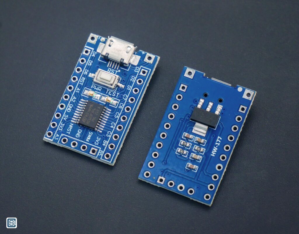
The STM8S103F3P6 is an 8-bit microcontroller from ST Microelectronics. It is basically a standalone 8-bit computer that can compute 8-bit wide numbers at a time. The specific chip variant comes in a 20-pin TSSOP package. It has 8 kilobytes (KB) of Flash memory to store all the instructions we provide. The flash storage is similar to the micro SD cards we use to store files. For the working memory, there is a 1 kilobyte of SRAM. Static Random Access Memory (SRAM) is a type of fast memory built using transistors. The advantage of an SRAM is that it is fast and allows random access to the memory locations. This is unlike the flash memory, which can only be accessed sequentially or as blocks of memory at a time. However, SRAMs are costly as they take more space on the chip die, due to which their sizes are limited on low-cost microcontrollers. Every CPU needs a clock source to drive its internal digital circuitry. The STM8S has an internal clock oscillator that can generate square wave signals of frequencies up to 16 MHz. For powering the microcontroller, you can use any DC voltage source with a voltage between 2.95 to 5.5V. Usually, we will power it from a 3.3V supply or a 5V supply.
The following are the reasons why we chose the STM8S for our basic microcontroller tutorial series.
- It is very cheap, nominally around INR 20 per piece.
- Global availability.
- Availability of supported open-source SDKs, frameworks, IDEs, and libraries.
- Comes with a two-wire debugging capability.
- Availability of cheap STM8 debuggers.
- Availability of cheap STM8S breakout boards.
STM8S has more features we want to discuss, but we can not explain all of them here at once. Instead, we will have dedicated tutorials for every feature of the STM8S and learn everything in detail. For now, we can skim over the specifications and block diagram of the STM8S103F3P6.
Specifications
- Core
- 16 MHz advanced STM8 core with Harvard architecture and 3-stage pipeline
- Extended instruction set
- Memories
- Program memory: 8 Kbyte Flash; data retention 20 years at 55 °C after 10 kcycle
- Data memory: 640-byte true data EEPROM; endurance 300 kcycle
- RAM: 1 Kbyte
- Clock, reset, and supply management
- 2.95 to 5.5 V operating voltage
- Flexible clock control, 4 master clock sources
- Low-power crystal resonator oscillator
- External clock input
- Internal, user-trimmable 16 MHz RC
- Internal low-power 128 kHz RC
- Clock security system with clock monitor
- Power management:
- Low-power modes (wait, active-halt, halt)
- Switch-off peripheral clocks individually
- Permanently active, low-consumption power-on and power-down reset
- Interrupt management
- Nested interrupt controller with 32 interrupts
- Up to 27 external interrupts on 6 vectors
- Timers
- Advanced control timer: 16-bit, 4 CAPCOM channels, 3 complementary outputs, dead-time insertion, and flexible synchronization
- 16-bit general purpose timer, with 3 CAPCOM channels (IC, OC or PWM)
- 8-bit basic timer with 8-bit prescaler
- Auto wake-up timer
- Window watchdog and independent watchdog timers
- Communication interfaces
- UART with clock output for synchronous operation, SmartCard, IrDA, LIN master mode
- SPI interface up to 8 Mbit/s
- I2C interface up to 400 kbit/s
- Analog to digital converter (ADC)
- 10-bit, ±1 LSB ADC with up to 5 multiplexed channels, scan mode, and analog watchdog
- I/Os
- Up to 28 I/Os on a 32-pin package including 21 high sink outputs
- Highly robust I/O design, immune against current injection
- Unique ID
- 96-bit unique key for each device
Block Diagram

The STM8 Core is where the CPU of this microcontroller sits. A Clock Controller provides the necessary timing signals for the CPU to operate. The Reset Block makes sure that the CPU starts with a known and predictable state when it is powered on, or upon the user’s request. Every other blocks are simply peripherals or memory sections the CPU can directly access. By reading and writing to the memory locations, the CPU can control the behaviour of the peripherals. We will learn about all of these peripherals and how you can write programs to interact with them. In the next tutorial, we will learn more about a basic STM8S103F3P6 breakout board and how to wire up one electrically. Check it out below.
The STM8S103F3P6 Development Board : Learn Microcontroller with STM8S – Tutorial Part #2
Links
Short Link
- Short URL to this page – https://www.circuitstate.com/whatismcustm8s

