The STM8S103F3P6 Development Board : Learn Microcontroller with STM8S – Tutorial Part #2
Learn about the internals of the STM8 microcontroller and learn how to design a minimum system development board like the STM8S-Blue.

In the last tutorial, we gave you an overview of the fundamentals of a microcontroller chip. In this tutorial, we will discuss more about the internals of the STM8S family of microcontrollers and the specific STM8S103F3P6 variant. We will also have a closer look at the STM8S-Blue microcontroller development board and how it is designed. If you have not read the first part of this tutorial, this is the best time to do it. Because more exciting tutorials are on the way that will give you hands-on knowledge of the world of microcontrollers.
What is A Microcontroller? : Learn Microcontroller with STM8S – Tutorial Part #1
Tutorial Series
- Learn the fundamentals of microcontrollers.
- Familiarize with a simple STM8S microcontroller.
- Install all the software tools and prepare your computer for programming and debugging microcontrollers.
- Get hands on experience with connecting your first microcontroller board and write a program for it.
- Learn the concepts of timers and interrupts in microcontrollers and blink an LED with what you learn.
- Learn how to make your microcontroller interact with the world by reading a push-button.
- Learn how to read a push-button using external interrupts without blocking critical code.
- Learn how to use the UART peripheral to print your first “Hello World” message to a computer.
What You’ll Learn
- How to design a minimum system development board for the STM8S103F3P6 microcontroller.
- The features and internal peripherals of the STM8S microcontroller.
STM8S Series
The STM8S is a series of low-cost and entry-level 8-bit microcontrollers from ST Microelectronics. The STM8S103F3P6 is one of many variants from this family. The name of all microcontrollers in this series start with STM8S which lets you identify which series a processor is. The following pictures show more products in this series with varying sets of features.


The product line-up is designed with software and pin compatibility in mind and a microcontroller with the same features will be available in different packages. This makes designing any electronic product with the STM8S microcontroller cost effective and future proof.
STM8S103F3P6
If you look at the product line-up image, the STM8S103F3xx is an access-line microcontroller available in 20-pin TSSOP or QFN packages. The last two characters of the product name indicate the package type. For example, P6 indicates the TSSOP-20 package which is an SMD package. TSSOP stands for Thin Shrink Small Outline Package which is one of the many standard packages used in the semiconductor industry. An SMD (Surface Mount Device) package is intended to be placed on the surface of a PCB. Therefore, there are no vertical pins on it. This also means that you can not directly connect an SMD package to a breadboard. We will see further how we can overcome this limitation.
Specifications
- Core
- 16 MHz advanced STM8 core with Harvard architecture and 3-stage pipeline
- Extended instruction set
- Memories
- Program memory: 8 Kbyte Flash; data retention 20 years at 55 °C after 10 kcycle
- Data memory: 640 byte true data EEPROM; endurance 300 kcycle
- RAM: 1 Kbyte
- Clock, reset and supply management
- 2.95 to 5.5 V operating voltage
- Flexible clock control, 4 master clock sources
- Low power crystal resonator oscillator
- External clock input
- Internal, user-trimmable 16 MHz RC
- Internal low-power 128 kHz RC
- Clock security system with clock monitor
- Power management:
- Low-power modes (wait, active-halt, halt)
- Switch-off peripheral clocks individually
- Permanently active, low-consumption power-on and power-down reset
- Interrupt management
- Nested interrupt controller with 32 interrupts
- Up to 27 external interrupts on 6 vectors
- Timers
- Advanced control timer: 16-bit, 4 CAPCOM channels, 3 complementary outputs, dead-time insertion and flexible synchronization
- 16-bit general purpose timer, with 3 CAPCOM channels (IC, OC or PWM)
- 8-bit basic timer with 8-bit prescaler
- Auto wake-up timer
- Window watchdog and independent watchdog timers
- Communication interfaces
- UART with clock output for synchronous operation, SmartCard, IrDA, LIN master mode
- SPI interface up to 8 Mbit/s
- I2C interface up to 400 kbit/s
- Analog to digital converter (ADC)
- 10-bit, ±1 LSB ADC with up to 5 multiplexed channels, scan mode and analog watchdog
- I/Os
- Up to 28 I/Os on a 32-pin package including 21 high sink outputs
- Highly robust I/O design, immune against current injection
- Unique ID
- 96-bit unique key for each device
Pinout
The pinout of a microcontroller lets us find what each pin is meant to be used for. There can be multiple VCC (VDD) or GND (VDD) pins, which should be connected together or connected as recommended by the datasheet. You can find all such information in the datasheet. For your easy reference, we will add the pinout here.

| Pin # | GPIO | High Sink | Speed | Main Alt. Function | Alt. Function |
|---|---|---|---|---|---|
| 1 | PD4 | HS | O3 | BEEP/TIM2_CH1/UART1_CK | – |
| 2 | PD5 | HS | O3 | AIN5/UART1_TX | – |
| 3 | PD6 | HS | O3 | AIN6/UART1_RX | – |
| 5 | PA1 | – | O1 | OSCIN | – |
| 6 | PA2 | – | O1 | OSCOUT | – |
| 10 | PA3 | HS | O3 | TIM2_CH3 | SPI_CS (AFR1) |
| 11 | PB5 | X | O1 | 12C_SDA | TIM1_ BKIN (AFR4) |
| 12 | PB4 | X | O1 | 12C_SCL | ADC_ETR (AFR4) |
| 13 | PC3 | HS | O3 | TIM1_CH3 | TLI (AFR3), TIM1_ CH1N (AFR7) |
| 14 | PC4 | HS | O3 | CLK_CCO/TIM1_CH4/AIN2 | TIM1_CH2N (AFR7) |
| 15 | PC5 | HS | O3 | SPI_SCK | TIM2_CH1 (AFR0) |
| 16 | PC6 | HS | O3 | SPI_COPI | TIM1_CH1 (AFR0) |
| 17 | PC7 | HS | O3 | SPI_CIPO | TIM1_CH2 (AFR0) |
| 18 | PD1 | HS | O4 | SWIM | – |
| 19 | PD2 | HS | O3 | AIN3 | TIM2_CH3 (AFR1) |
| 20 | PD3 | HS | O3 | AIN4/TIM2_CH2/ADC_ETR | – |
- Only GPIO pins are shown.
- Default function of all GPIO pins after reset is port GPIO.
- – – Not applicable
- X – Not available
- Ox – Speed Class
- O1 – Slow (up to 2 MHz)
- O2 – Fast (up to 10 MHz)
- O3 – Fast/slow programmability with slow as default state after reset
- O4 – Fast/slow programmability with fast as default state after reset
The default function of most of the pins other than power pins is the GPIO (General Purpose Input/Output) function. GPIO is a mode where you can drive a pin to a HIGH or LOW states which correspond to the binary 1 and 0 respectively. In addition to that, each pin can have alternate functions which we can set using the internal configuration registers. Only one function should be active at a time. We will learn how you can configure the GPIO pins and their functions in the upcoming posts. For now, you just need to keep the pinout table as a handy reference.
Block Diagram
Following is a general block diagram of the STM8 series which shows all of the features available in the series.

Following is the specific block diagram of the STM8S103F3P6. We have seen this block diagram in the Part #1 of this tutorial. But we did not explain all of the internal blocks in details. We will now give you brief descriptions of each of the blocks found inside the MCU block diagram. We will learn about all of the modules in-depth in the upcoming tutorials.

Reset
The Reset block inside a microcontroller helps the entire system to get initialized with a known state. Without a proper reset mechanism, each of the logical blocks of the microcontroller might initialize to random states and therefore cause unpredictability in the operation. For example, a register called Program Counter (PC) stores the memory location of the next instruction to be executed. If this register is initialized with random values every time we power on the system, our application code will never be executed correctly. There are a few ways to initiate a system reset, including a external reset input pin (NRST).

POR
Power-On Reset (POR) is triggered when power is applied to the microcontroller. When the power supply is connected, it can take a small amount of time for the supply voltage to stabilize. The POR mechanism makes sure that the microcontroller is reset after the power supply is stable. So every time you apply power to the microcontroller, it initializes to the same predictable state.
BOR
A Brown-Out Reset (BOR) is triggered when the power supply becomes unstable. This can happen when the voltage drops below the working voltage range of the microcontroller. If the supply voltage is not sufficient, the internal digital circuits can not work properly, which can drive them to unpredictable states. The brown-out voltage for a microcontroller will be mentioned in the datasheet. For proper operation, you have to make sure that the supply voltage never goes below the threshold voltage. Most modern microcontrollers have a register that tells if your microcontroller has been reset due to a brown-out.

Manual
A manual reset can be triggered from an external pin or by a software instruction. For externally resetting an STM8S microcontroller, you can use the NRST pin. The default state of this pin will be in pulled-up (pin connected to positive voltage with a high value resistor) state. Whenever the state of the pin becomes LOW for a sufficient period, a reset is triggered.
A software reset can be triggered by a reset instruction added in the application code. When the instruction is executed, the MCU is reset and starts executing the code from the start of the program as normal.
Clock Controller
A Clock Controller generates and supplies various frequencies of clock signals to different parts of a microcontroller. Not all parts of the MCU run at the same speed. The Clock Controller will generate a base clock (a square wave signal) from an oscillator circuit. For sections that require a higher frequency than the base clock, frequency multipliers (such as PLLs) are used. For parts that require lower frequencies, frequency dividers are used. Some of the frequency multipliers and dividers are programmable via registers which allows you to set the exact frequency you need for a particular application.

STM8 Core
We do not have a complete internal working of an STM8 core since the manufacturer keeps that as a proprietary information. Nevertheless, the function of an 8-bit CPU will be more or less the the same in the perspective of a computer programmer. This perspective is usually called the Programmer’s Model. We have seen how a generic 8-bit computer works in the previous tutorial. So we will not go in depth about the core at this time. Instead, we will explain everything you want to know on the fly.
WDT/WDG
A Watchdog Timer is a circuit that runs independent of the CPU. It’s primary function is to trigger a reset of the microcontroller when it gets stuck due to a logical error in the program. The error can happen due to a logical error in the program that only happens at run-time or can be a bit-flip. Without a reset trigger, the microcontroller will be stuck in the state forever until the power is disconnected or a manual reset is triggered. WDT saves critical systems from random failures and allow them to restart fresh and thus recovering from the lockout. A WDT is usually a digital counter that listens for a heartbeat (a periodic signal from the CPU that tells it is in a working state) signal which resets the WDT periodically. If the WDT is not reset after a certain period, it will trigger a hard reset causing the microcontroller to execute the program from the start.

Flash
A Flash is a type of non-volatile memory (contents of the memory are not lost when powered down) that is typically used to store the program written by the user. Most microcontrollers come with integrated Flash memory of a few kilobytes to many megabytes. Some MCUs can be interfaced with external Flash memory chips of different capacities. Flash memories are slower than a RAM but also cheaper. Flash memories can be read and written multiple times, but most of them have a lifespan expressed in the number of erase cycles after which they start to degrade. But this life span is usually in the ranges of multiple thousands. So nothing to be worried about outright.

EEPROM
An Electronically Erasable Programmable Memory (EEPROM) is a mouthful word for another type of memory. An EEPROM is similar to a Flash memory but has more data retention span than a typical Flash memory. Also, EEPROMs usually have a lower write cycle life compared to Flash memory. EEPROMS are commonly used for storing configuration parameters that do not change often. These days, Flash memories are used just like EEPROMs and so it is not necessary to have dedicated EEPROMs.
RAM
A Random Access Memory, as the name implies, allows random access of its memory contents. But why does having random access matter at all? Memories are actually large circuits with repeating blocks. Accessing one location of the memory may not take the same time as accessing another location. Another fact is that not all memories can be accessed as individual bits or bytes, but instead can only be accessed as a set of locations commonly called sectors or pages. For a CPU to carry out its task, it needs to access all of the memory locations with consistent timings and as fast as possible. It also needs to access the memory locations in byte or bit addressing modes. Microcontroller RAMs are usually made of transistor-based flip-flops which are called Static RAM (SRAM).

Debug/SWIM
Debugging is the process of finding and fixing issues in a computer program. An issue in a program is commonly called a bug and debugging refers to fixing the bugs. Not all issues in your code may be obvious at a first look. Some issues can only be identified by running the system and observing when and where it fails. Debugging process allows us to see the hardware closer when it is running, and see the register values and other states in real-time. There exists multiple standards and interfaces for debugging microcontroller and the Single Wire Interface Module (SWIM) is what is available in the STM8S microcontrollers. We will learn to use this interface in the future.

I2C
Inter-Integrated Circuit (I2C, commonly pronounced as “I two C” or “I squared C”) is a popular serial data communication standard and protocol. It is a synchronous communication interface with a dedicated clock line shared by all devices. It was developed by Philips and uses only two wires for bidirectional communication, other than a common ground. The advantage of I2C is that it is a “bus” where multiple devices can communicate at the same time. This is in contrast to point-to-point communication interfaces where one device communicates to another device exclusively (e.g. UART). I2C has two lines, Serial Data (SDA) and Serial Clock (SCL). Devices can only transmit or receiver at a time, which makes it half-duplex in nature. I2C is commonly used for interfacing sensors and provides data rates of 100 kbps to 1 Mbps.

SPI
The Serial Peripheral Interface (SPI) is another common standard for serial data communication. Unlike I2C, it needs more number of wires and it is also not a bus. Even though multiple devices can share multiple common signals, only one device can be active at a time which is controlled using a dedicated Chip Select (CS) line. Even though this might seem like a disadvantage, the power of SPI lies in its fast and reliable data transfers. The reliability comes from dedicated and shared clock line (SCK) and directional data lines (COPI & CIPO). The dedicated clock line also makes SPI a synchronous interface. SPI is a full-duplex interface commonly used to interface memories and other high-bandwidth peripherals such as displays and cameras.
UART
UART (Universal Asynchronous Receiver Transmitter) is a very popular serial communication standard. In fact, if you hear the term serial communication anywhere, it is highly likely to be a UART serial interface. As the name says, UART is asynchronous, which means there is no dedicated clock lines shared between the participating devices. Instead, each device must agree to use a common data rate (typically called a baud rate). If the sending and receiving baud rates are different, the communication won’t be sensible. UART is a full-duplex communication interface with dedicated receiver (RX) and transmit (TX) lines.
ADC
An Analog to Digital Converter (ADC) converts continuous analog voltages into digital (binary) values. Since almost all of the physical quantities such as temperature, pressure, light, etc. can be converted to electrical voltage, microcontrollers can measure physical quantities with the help of ADCs. An ADC can accept a range of voltage through one of the microcontroller pins and convert it to a binary value that we can use in the program. The STM8S comes with a 10-bit ADC with 5 channels. Each channel represents a pin and you can read different voltage levels through up to 5 pins. A 10-bit resolution can convert an input with a 3.22 mV precision.
Beeper
The STM8 microcontroller contains a dedicated peripheral for driving external beepers. This saves the programmer from writing timing loops or using precious timers to drive simple beepers. The beeper driver can produce 1/2/4 kHz of signals to produce the same frequency of sound.

Timer
Timers and Counters are universal features of all microcontrollers. The timer inside a microcontroller is a digital circuit that either produces timing signals or counts an input signal. Timers are used when we want to generate precise rectangular signals (square wave included) without actually using the CPU to switch a GPIO pin. We can simply load the timer with a preset value and whenever the timer overflows, it will produce an interrupt signal and reload the timer with the preset value again. We will learn more about timers and counters in our programming tutorial.
Address & Data Bus
The Address and Data bus is a fabric of circuits inside the microcontroller that helps the various peripherals to communicate each other. It is an information highway inside the chip. All peripherals have their associated registers or memories, with unique memory addresses assigned to them. Whenever the CPU wants to communicate with a peripheral, it can simply assert the memory address on the Address bus and get that data through the Data bus. The access to buses is controlled by various methods including multiplexing.
STM8S-Blue
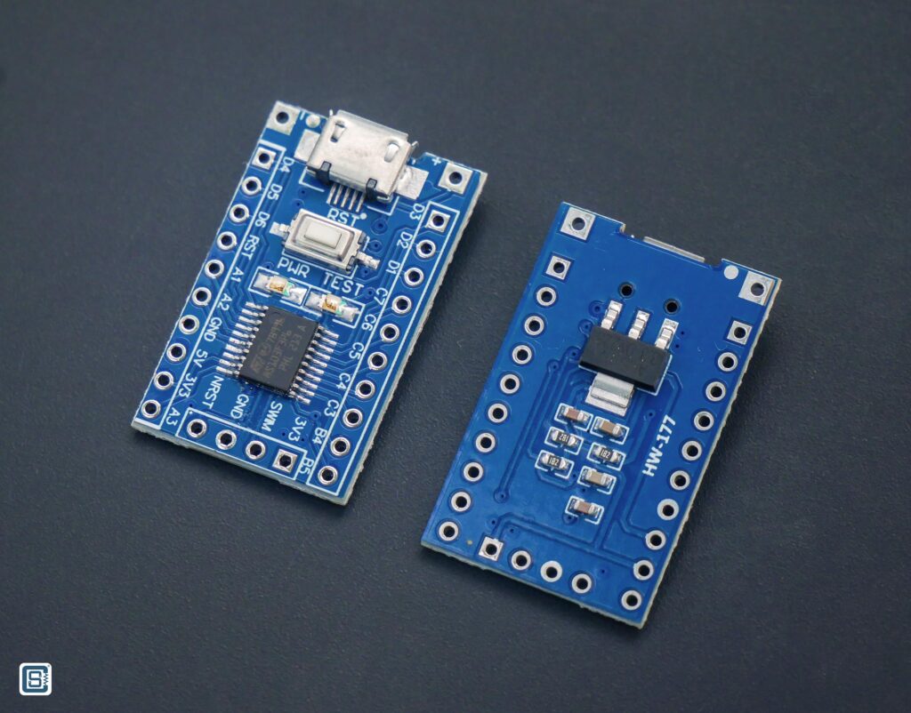
Manufacturers produce microcontrollers in various standard IC packages that we can solder on a PCB. Microcontrollers in through-hole (THT – Though-Hole Technology) package can be easily placed on a breadboard and be connected to other electronic components. But the surface-mount (SMT – Surface Mount Technology) microcontrollers need to be soldered on a PCB or soldered with tiny wire to be able to use it. To overcome the difficulty, many manufacturers produce breakout boards that contain the MCU and a few other components that are necessary to get the MCU working. These boards are usually called Minimum System Development Board. The STM8S-Blue is such a board for the STM8S103F3P6 microcontroller that we are going to use in this tutorial series. It is a generic and cheap board widely available from different vendors. You can get the board for INR 300 or less in India. It is one of the reasons why we decided to use the STM8S for our first microcontroller tutorial series.
Specifications
| Specification | Value |
|---|---|
| CPU | STM8S103F3P6 |
| Series | STM8S |
| Clock | 16 MHz (Internal) |
| Flash | 8 kB |
| RAM | 1 kB |
| EEPROM | 640 bytes |
| I/O voltage | 3.3V |
| GPIO | 14 |
| Interface ports | UART, SPI, I2C |
| PWM | 4 (up to 7 via alternate mapping) |
| ADC | 5-channel, 10-bit |
| LED | PB5 (Arduino D3), active low, shared with I2C, red |
| Program/Debug Interface | SWIM |
| USB | Micro-USB (power only) |
| Dimensions | 18 x 30 mm |
Schematic
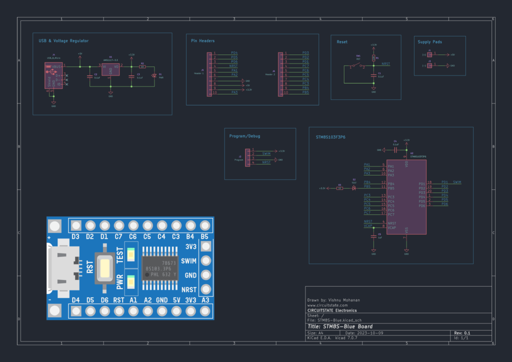
The most essential part of the schematic is the power supply section. The USB-Micro connector will receive 5V from a PC or some other device. The AMS1117 voltage regulator will convert the 5V to 3.3V for the MCU. Applying 5V directly to the MCU will not damage it since the working voltage of the STM8S microcontroller is from 2.5V~5.5V. The absolute maximum rating is 6.5V. So if you don’t exceed that voltage, you won’t damage the MCU. Regardless of the input voltage, the CPU will always run with a 1.8V generated internally. We can understand this better by looking at the following power diagram of STM8S.

Note that all of what is shown here resides inside the chip, not outside of it. The internal Main Voltage Regulator will convert the input voltage supplied to the VDD pin to a 1.8V for the CPU, RAM and Flash memory. The ADC has a separate supply line VDDA where you can connect a low-noise power supply. The VDDIO pin is what accepts the voltage for the GPIO pins and other peripherals. In the STM8S, the VDDA and VDDIO pins are not broken out separately, but internally connected together. So we can supply all of them through the single VDD pin. 1.8V, 2.5V, 3.3V and 5V are standard voltages in the embedded industry. Normally, when we design an embedded system, the voltages and the power supply types are determined according to the requirements. When designing a generic system, the system voltage is kept at one of the standard or well-known voltage levels. This is why we are using 3.3V here and using an external voltage regulator for it. The voltage regulator will also reduce the noise coming from the input side and also protect the MCU from overvoltages.
Apart from the voltage regulator, there is an LED labelled as PWR to indicate when the power is on. A momentary push-button labelled as RST is connected to the NRST pin of the MCU. Pressing this button will trigger a manual reset of the MCU. The 0.1 uF capacitor allows the reset pin to remain in the LOW condition for enough time. Without the capacitor, the reset won’t be proper. An LED labelled as TEST is connected to the PB5 GPIO pin for debugging purposes. We can test the MCU by blinking the LED in this case. The 1K resistor will limit the current through the LED. Everything else you see on the schematic are just breakout pin headers that expose various IO pins and other signals. For example, B4 indicates the GPIO pin PB4. If you ever want to use an STM8S microcontroller in your application, you can use this circuit as the reference.
Pinout
The pinout list tells you what function can be assigned to each of the GPIO pins of the microcontroller. We have created a beautiful vector pinout diagram for the STM8S-Blue board. Keep this list handy for quick reference when you are programming.
STM8S-Blue Generic STM8S103F3P6 Development Board – Pinout Diagram & Pin Reference
What’s Next?
We hope you got a good overview of the STM8S103F3P6 microcontroller and the STM8S-Blue board. In the next tutorial, we will start setting up the development environment and writing programs for the microcontroller and learn how to use all of the features of the microcontroller. To follow the tutorial, you will need to get the below listed items, if you don’t already have them. We will add links to a store for your reference, but you can buy it from anywhere else that is cheaper.
- STM8S-Blue Board
- USB-Micro Cable
- ST-Link V2 STM32 Programmer & Debugger (the clone is enough)
- Breadboard
- Jumper Cables (All three types)
Check out the next part of this tutorial series below.
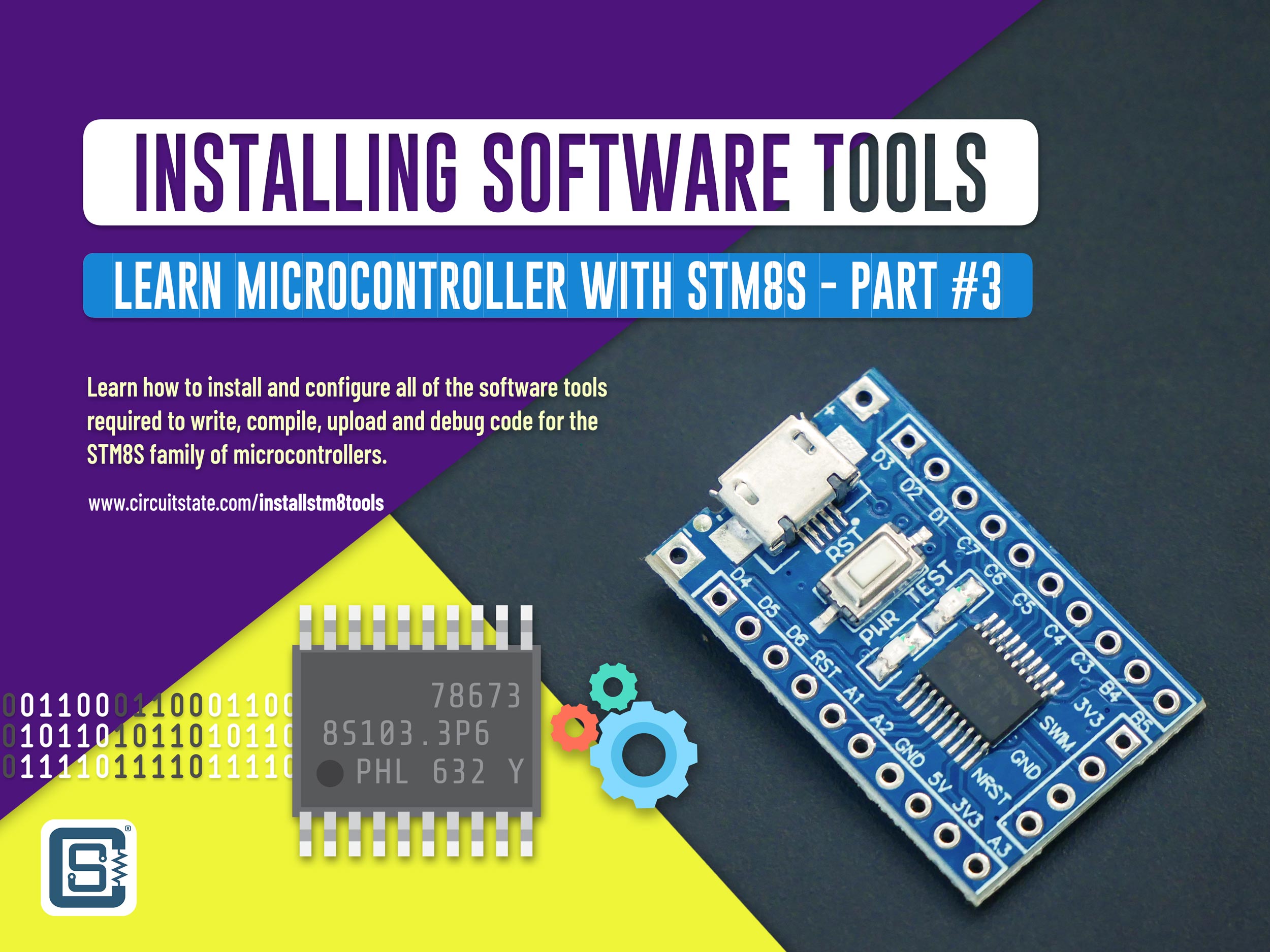
Installing Development Tools : Learn Microcontroller with STM8S – Tutorial Part #3
Links
- What is A Microcontroller? : Learn Microcontroller with STM8S – Tutorial Part #1 – CIRCUITSTATE Electronics
- STM8S Series – Official Product Page
- STM8S103F3 Datasheet [PDF]
- AN2752 – Getting Started with STM8S and STM8AF Microcontrollers [PDF]
- PM0044 – STM8 CPU Programming Manual [PDF]
- RM0016 – STM8S and STM8AF Series 8-Bit Microcontrollers [PDF]
- STM8 Product Lineup [PDF]
- Buy STM8S Blue Board – Robu.in
Short Link
- A short URL to this page – https://www.circuitstate.com/stm8sblueboard


