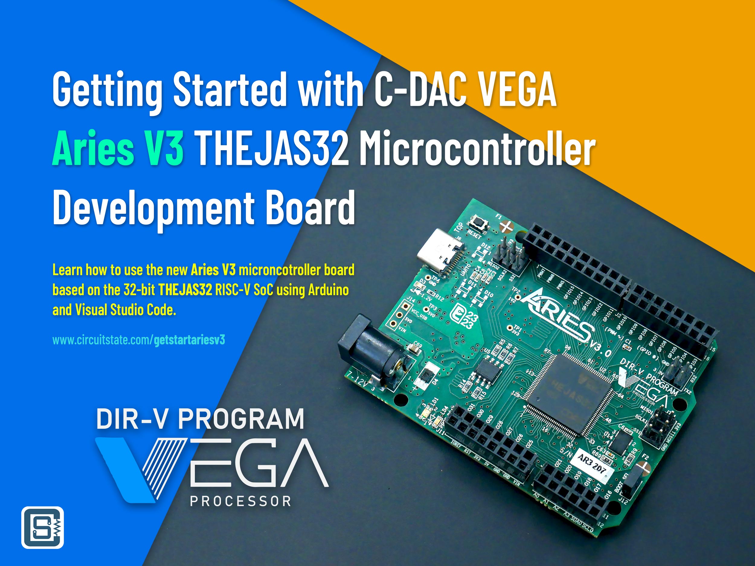
C-DAC Aries V3 THEJAS32 Microcontroller Board – Pinout Diagram & Pin Reference

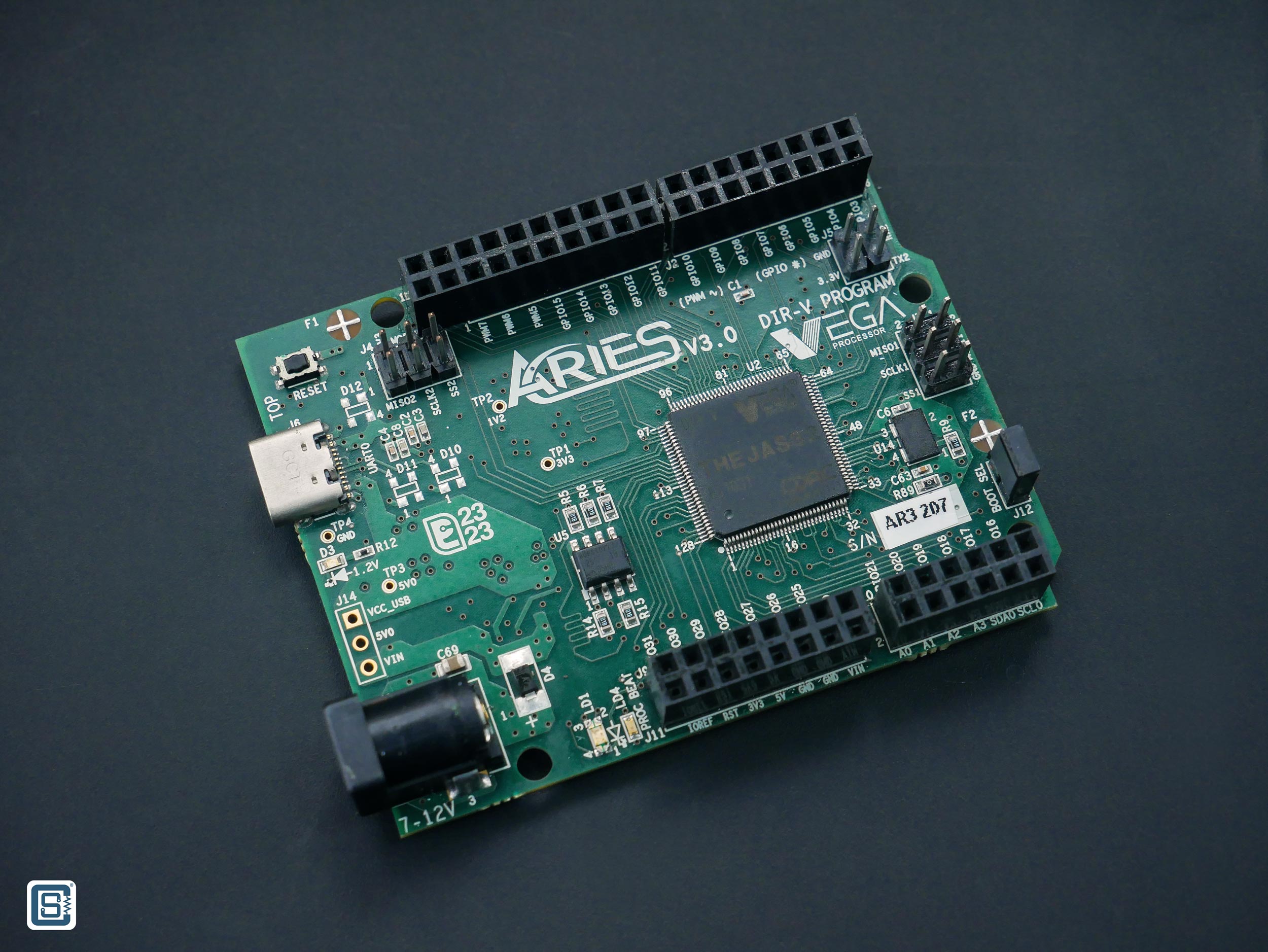
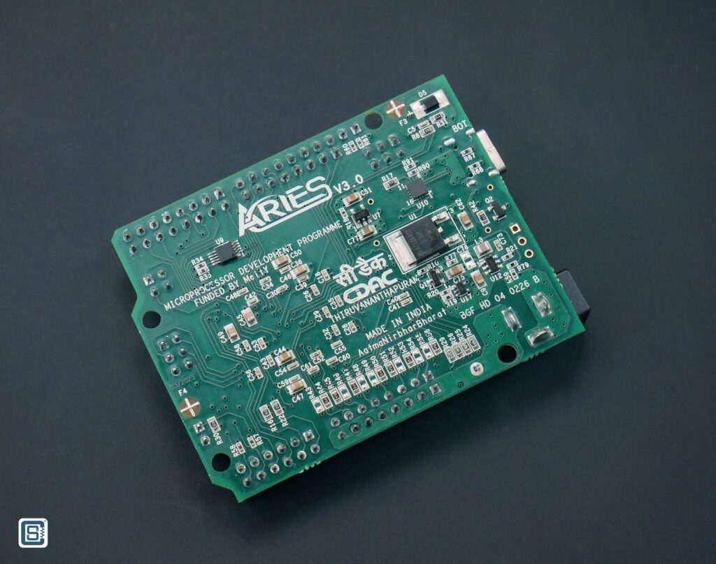
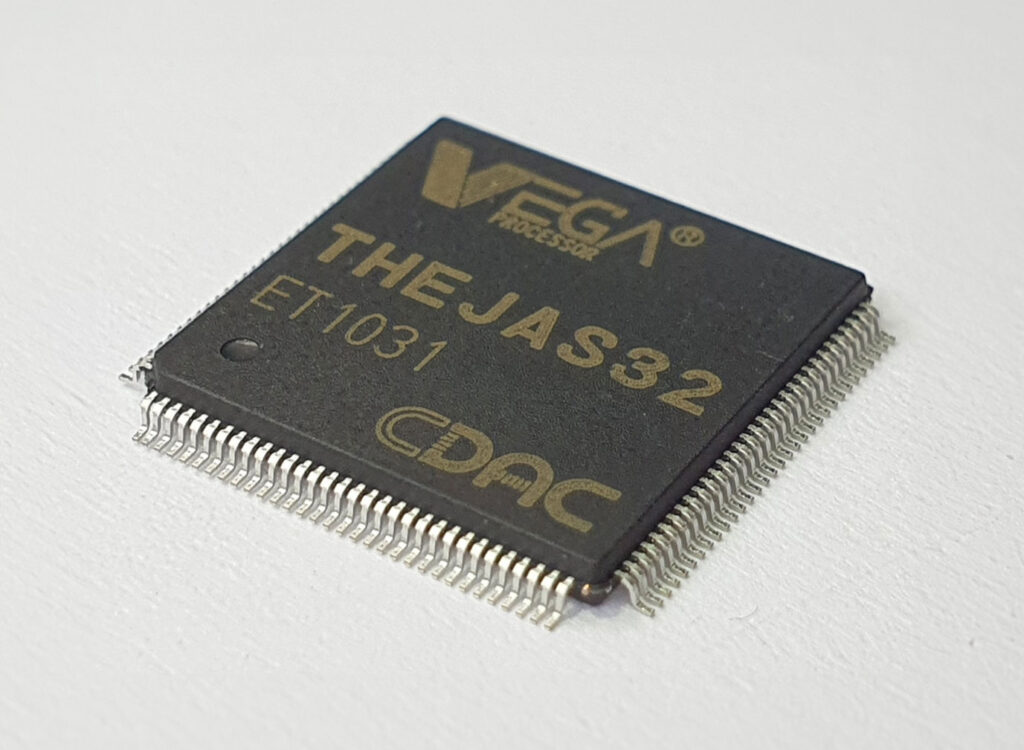
Aries V3 is a THEJAS32 SoC development board by C-DAC (Centre for Development of Advanced Computing, India). The microcontroller SoC and the board are a result of the DIR-V program funded by the Ministry of Electronics and Information Technology (MeitY), Government of India. The THEJAS32 SoC integrates a 32-bit single-core VEGA ET1031 RISC-V CPU that runs at 100 MHz. The SoC is available as a 128-pin LQFP package. The Aries V3 board is the third version of THEJAS32-based boards. It is the cheapest one in the family and gives you a bare minimum system for development. The Aries V3 is designed in the same form factor as an Arduino Uno with pin compatibility. On this page, you will find a vector pinout diagram, Arduino pin reference and other useful information for the Aries V3 board.
Aries V3
If you are new to Aries V3 and the THEJAS32 microcontroller, we have a tutorial to get you started. You can use the Arduino IDE or VS Code to develop applications for your Aries V3 boards.
Getting Started with C-DAC Aries V3 THEJAS32 Microcontroller Development Board
Specifications
| Specification | Value |
|---|---|
| Microcontroller | THEJAS32 SoC |
| Microprocessor Core | 32-bit VEGA ET1031 |
| Core Count | 1 |
| SRAM | 256 KB |
| Flash | 2MB (External) |
| Input Voltage | 7-12V |
| USB | USB-C |
| PWM Pins | 8 |
| Analog Input Pins | 4 |
| SPI | 3 |
| UART | 3 |
| I2C | 2 |
| GPIOs | 32 |
| DC Current per I/O Pin | 12 mA |
| IO Voltage | 3.3V |
| Clock Speed | 100 MHz |
| Length | 78 mm |
| Width | 66 mm |
Board Topology
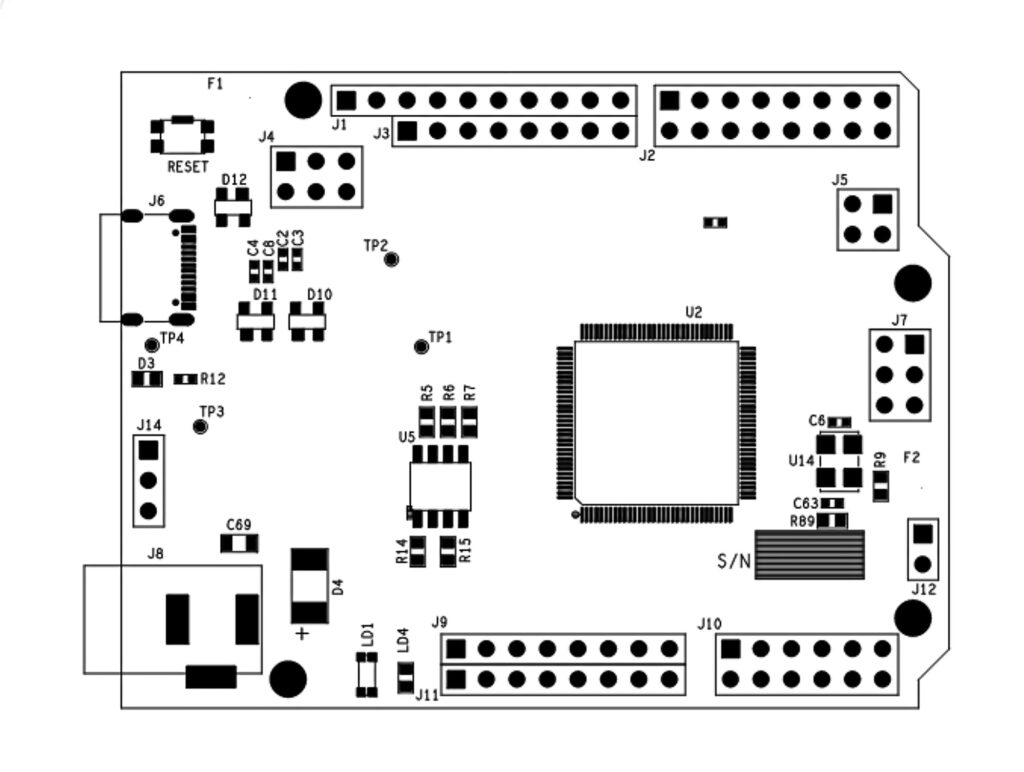
| Reference | Description |
|---|---|
| J5 | UART |
| J7 | SPI1 |
| J4 | SPI2 |
| J8 | Power Jack |
| J6 | USB-C Connector |
| J12 | Boot Select Header |
| J14 | Power Header |
| RESET | Reset Button |
| LD1 | RGB LED |
| LD4 | Processor HeartBeat LED |
| U2 | THEJAS32 SoC |
| U1 | 3.3V Regulator |
| U4 | 100 MHz Oscillator |
| U5 | SPI Boot Flash Memory |
| U6 | Op-amp |
| U7 | 1.2V Regulator |
Pinout Diagram
Latest Revision: Rev 0.1, 23-10-2023
Design by: Vishnu Mohanan
License: CC-BY-SA 4.0
The pinout diagram is based on the official documents. While we try our best to be accurate and up-to-date here, we can not guarantee correctness. We have seen boards with conflicting pinouts and pin labels. So please also double-check the pin assignments with that from the official documentation. If you find any errors, please let us know in the comments.
PNG
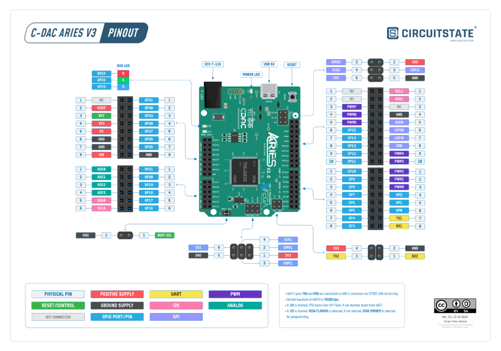
PDF preview may not load on mobile devices. Click the link to open an interactive preview, or download it directly.
Pin Reference
[TODO]
THEJAS32 SoC
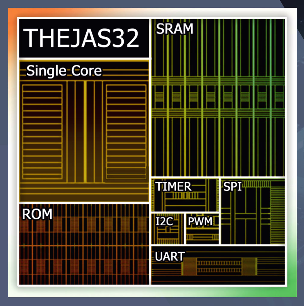
Specifications
The key specs of the THEJAS32 SoC are,
- 32-bit Single-core RISC-V
- Clock Speed: 100 MHz
- 256 KB SRAM
- Upto 16 MBit Flash
- 8x PWM pins
- 4x Analog input pins
- 3x SPI
- 3x UART
- 2x I2C
- Upto 25 GPIOs
- Input Voltage: 7-12V
- DC Current per I/O Pin: 12 mA
- IO Voltage: 3.3 V
- Package: LQFP-128
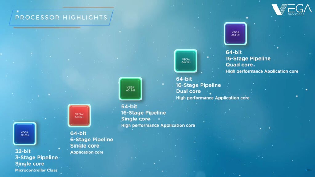
The key features of the VEGA ET1031 processor core are,
- RISC-V (RV32IM) Instruction Set Architecture
- 3-stage in-order pipeline implementation
- Harvard architecture (separate instruction and data buses)
- High-performance multiply/divide unit
- Configurable AXI4 or AHB external interface
- Optional MPU (Memory Protection Unit)
- Platform Level Interrupt Controller
- Up to 127 IRQs
- Low interrupt latency
- Vectored interrupt support
- Advanced Integrated Debug Controller
- Debug extension allowing Eclipse debugging via a GDB–openOCD–JTAG connection
Pinout
| Pin # | Pin Name | Description |
|---|---|---|
| 1 | GPIO1(3) | General purpose IO. |
| 2 | GPIO1(2) | General purpose IO. |
| 3 | PVSSIOC23 | Ground reference for IO pins. |
| 4 | PVDDIO23 | Positive supply for IO pins. Connect to 3.3V supply. |
| 5 | GPIO1(1) | General purpose IO. |
| 6 | GPIO1(0) | General purpose IO. |
| 7 | SPI3MOSI | SPI 3 Master Out Slave In. |
| 8 | PVDDC18 | Positive supply for logic. Connect to 1.2V supply. |
| 9 | PVSSC18 | Ground reference for logic. |
| 10 | SPI3MISO | SPI 3 Master In Slave Out. |
| 11 | SPI3CLK | SPI 3 Clock. |
| 12 | SPI3CSN | SPI 3 Chip Select. |
| 13 | PVSSIOC21 | Ground reference for IO pins. |
| 14 | PVDDIO21 | Positive supply for IO pins. Connect to 3.3V supply. |
| 15 | BOOT | Boot select. |
| 16 | PROCBT | Heartbeat signal. |
| 17 | TEDTUPD | Connect to GND. |
| 18 | PVDDC17 | Positive supply for logic. Connect to 1.2V supply. |
| 19 | PVSSC17 | Ground reference for logic. |
| 20 | TSTCLK | Connect to GND through a 1K resistor. |
| 21 | TJTAGTDO | JTAG TDO. Left unconnected. |
| 22 | TJTAGTMS | JTAG TMS. Connect to GND through a 1K resistor. |
| 23 | TJTAGTDI | JTAG TDI. Connect to GND through a 1K resistor. |
| 24 | PVSSIOC19 | Ground reference for IO pins. |
| 25 | PVDDIO19 | Positive supply for IO pins. Connect to 3.3V supply. |
| 26 | PVDDC16 | Positive supply for logic. Connect to 1.2V supply. |
| 27 | PVSSC16 | Ground reference for logic. |
| 28 | TJTAGTCK | JTAG TCK. Connect to GND through a 1K resistor. |
| 29 | TJTAGTRST | JTAG TRST. Connect to GND through a 1K resistor. |
| 30 | TSTMODE | Test mode select. Connect to GND through a 1K resistor. |
| 31 | IIC2SDA | I2C 2 Serial Data. |
| 32 | IIC2SCL | I2C 2 Serial Clock. |
| 33 | IIC0SCL | I2C 0 Serial Clock. |
| 34 | IIC0SDA | I2C 0 Serial Data. |
| 35 | PVSSC14 | Ground reference for logic. |
| 36 | PVDDC14 | Positive supply for logic. Connect to 1.2V supply. |
| 37 | PVDDIO17 | Positive supply for IO pins. Connect to 3.3V supply. |
| 38 | PVSSIOC17 | Ground reference for IO pins. |
| 39 | SPI1CSN | SPI 1 Chip Select. |
| 40 | SPI1CLK | SPI 1 Clock. |
| 41 | SPI1MISO | SPI 1 Master In Slave Out. |
| 42 | SPI1MOSI | SPI 1 Master Out Slave In. |
| 43 | RSTIN | Reset. |
| 44 | CLKSYS | System Clock. |
| 45 | URT1SOUT | UART 1 Serial Out/Transmit. |
| 46 | PVDDIO15 | Positive supply for IO pins. Connect to 3.3V supply. |
| 47 | PVSSIOC15 | Ground reference for IO pins. |
| 48 | PVSSC12 | Ground reference for logic. |
| 49 | PVDDC12 | Positive supply for logic. Connect to 1.2V supply. |
| 50 | URT1SIN | UART 1 Serial Receive. |
| 51 | GPIO0(15) | General purpose IO. |
| 52 | GPIO0(14) | General purpose IO. |
| 53 | GPIO0(13) | General purpose IO. |
| 54 | GPIO0(12) | General purpose IO. |
| 55 | GPIO0(11) | General purpose IO. |
| 56 | PVSSC11 | Ground reference for logic. |
| 57 | PVDDC11 | Positive supply for logic. Connect to 1.2V supply. |
| 58 | GPIO0(10) | General purpose IO. |
| 59 | PVDDIO13 | Positive supply for IO pins. Connect to 3.3V supply. |
| 60 | PVSSIOC13 | Ground reference for IO pins. |
| 61 | GPIO0(9) | General purpose IO. |
| 62 | GPIO0(8) | General purpose IO. |
| 63 | GPIO0(7) | General purpose IO. |
| 64 | GPIO0(6) | General purpose IO. |
| 65 | GPIO0(5) | General purpose IO. |
| 66 | GPIO0(4) | General purpose IO. |
| 67 | PVSSC9 | Ground reference for logic. |
| 68 | PVDDC9 | Positive supply for logic. Connect to 1.2V supply. |
| 69 | PVDDIO11 | Positive supply for IO pins. Connect to 3.3V supply. |
| 70 | PVSSIOC11 | Ground reference for IO pins. |
| 71 | GPIO0(3) | General purpose IO. |
| 72 | GPIO0(2) | General purpose IO. |
| 73 | GPIO0(1) | General purpose IO. |
| 74 | GPIO0(0) | General purpose IO. |
| 75 | PWM(7) | Pulse Width Modulation. |
| 76 | PWM(6) | Pulse Width Modulation. |
| 77 | PWM(5) | Pulse Width Modulation. |
| 78 | PVSSC7 | Ground reference for logic. |
| 79 | PVDDC7 | Positive supply for logic. Connect to 1.2V supply. |
| 80 | PWM(4) | Pulse Width Modulation. |
| 81 | PWM(3) | Pulse Width Modulation. |
| 82 | PWM(2) | Pulse Width Modulation. |
| 83 | PVDDIO8 | IO Power Supply VDD pin. |
| 84 | PVSSIOC8 | Ground reference for IO pins. |
| 85 | PWM(1) | Pulse Width Modulation. |
| 86 | PWM(0) | Pulse Width Modulation. |
| 87 | SPI0MOSI | SPI 0 Master Out Slave In. |
| 88 | PVSSC6 | Ground reference for logic. |
| 89 | PVDDC6 | Positive supply for logic. Connect to 1.2V supply. |
| 90 | SPI0MISO | SPI 0 Master In Slave Out. |
| 91 | SPI0CLK | SPI 0 Clock. |
| 92 | SPI0CSN | SPI 0 Chip Select. |
| 93 | PVDDIO6 | Positive supply for IO pins. Connect to 3.3V supply. |
| 94 | PVSSIOC6 | Ground reference for IO pins. |
| 95 | IIC1SDA | I2C 1 Serial Data. |
| 96 | IIC1SCL | I2C 1 Serial Clock. |
| 97 | SPI2MOSI | SPI 2 Master Out Slave In. |
| 98 | SPI2MISO | SPI 2 Master In Slave Out. |
| 99 | PVDDC4 | Positive supply for logic. Connect to 1.2V supply. |
| 100 | PVSSC4 | Ground reference for logic. |
| 101 | SPI2CLK | SPI 2 Clock. |
| 102 | SPI2CSN | SPI 2 Chip Select. |
| 103 | PVSSIOC4 | Ground reference for IO pins. |
| 104 | PVDDIO4 | Positive supply for IO pins. Connect to 3.3V supply. |
| 105 | URT2SIN | UART 2 Serial In Receive. |
| 106 | URT2SOUT | UART 2 Serial Out / Transmit. |
| 107 | URT0SIN | UART 0 Serial In Receive. |
| 108 | URT0SOUT | UART 0 Serial Out / Transmit. |
| 109 | GPIO1(15) | General purpose IO. |
| 110 | GPIO1(14) | General purpose IO. |
| 111 | GPIO1(13) | General purpose IO. |
| 112 | PVDDC2 | Positive supply for logic. Connect to 1.2V supply. |
| 113 | PVSSC2 | Ground reference for logic. |
| 114 | PVSSIOC2 | Ground reference for IO pins. |
| 115 | PVDDIO2 | Positive supply for IO pins. Connect to 3.3V supply. |
| 116 | GPIO1(12) | General purpose IO. |
| 117 | GPIO1(11) | General purpose IO. |
| 118 | GPIO1(10) | General purpose IO. |
| 119 | GPIO1(9) | General purpose IO. |
| 120 | GPIO1(8) | General purpose IO. |
| 121 | GPIO1(7) | General purpose IO. |
| 122 | GPIO1(6) | General purpose IO. |
| 123 | PVSSIOC0 | Ground reference for IO pins. |
| 124 | PVDDIO0 | Positive supply for IO pins. Connect to 3.3V supply. |
| 125 | PVDDC0 | Positive supply for logic. Connect to 1.2V supply. |
| 126 | PVSSC0 | Ground reference for logic. |
| 127 | GPIO1(5) | General purpose IO. |
| 128 | GPIO1(4) | General purpose IO. |
Links
- Aries V3 Product Page – C-DAC
- Aries V3 Datasheet [PDF]
- THEJAS32 SoC Borchure [PDF]
- VEGA User Guide
- VEGA SDK User Guide
- C-DAC – Official Website
Short Link
- Short URL to this page – https://www.circuitstate.com/ariesv3pins
