Waveshare ESP32-S3-DEV-KIT-NxR8 Wi-Fi Development Board – Pinout Diagram & Arduino Reference
Complete pinout reference for the Waveshare ESP32-S3-DEV-KIT-NXR8 ESP32-S3 Wi-Fi development board including Arduino pin and interface references.
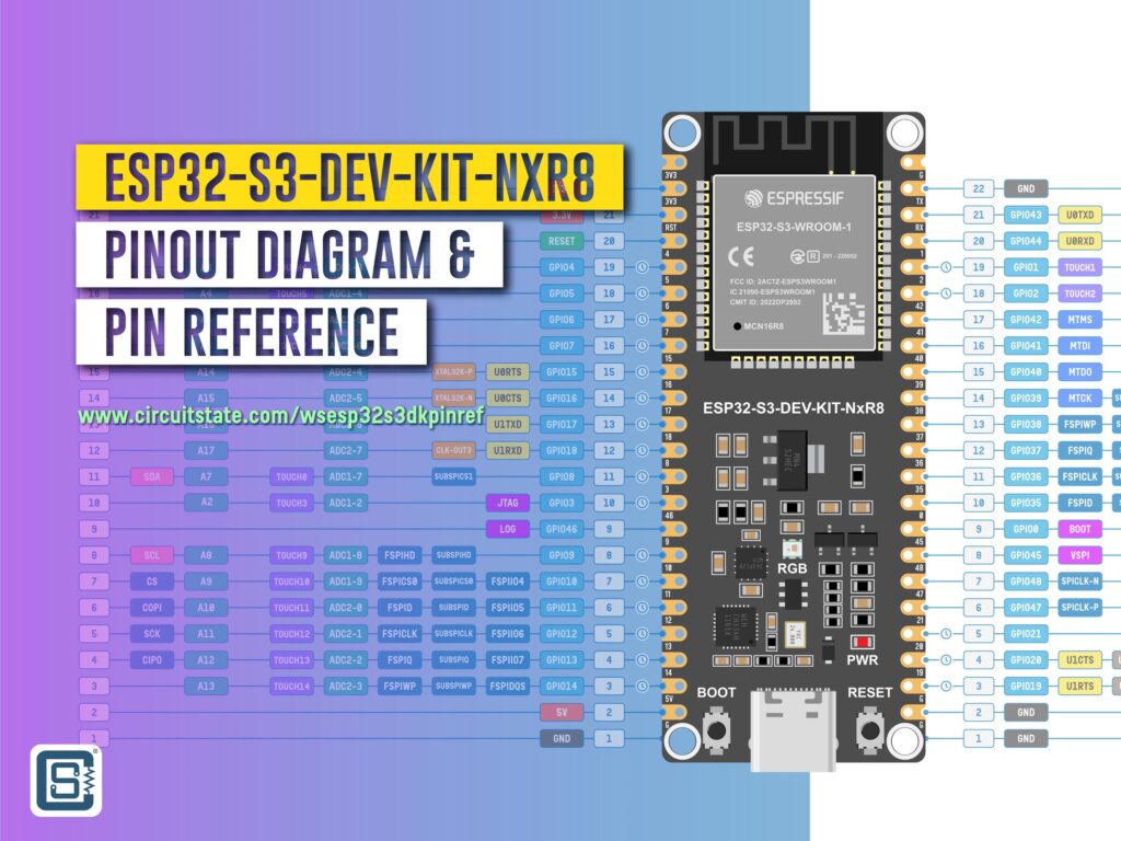
After the enormous success of the ESP32 microcontroller, Espressif released an upgraded version of it called the ESP32-S3. The new ESP32-S3 overcomes many shortcomings of the legacy ESP32. Today, there are hundreds of boards designs based around the ESP32-S3 in the market as well as in the open-source community. In this post we are going to share a beautiful vector pinout diagram for the ESP32-S3-DEV-KIT-NxR8 development board from Waveshare. The board is designed after the official ESP32-S3_DevKitC-1 from Espressif. So the pinouts you see here also applies to that. If you are new to the ESP32-S3 Wi-Fi and Bluetooth SoC, we have a great tutorial to get you started.
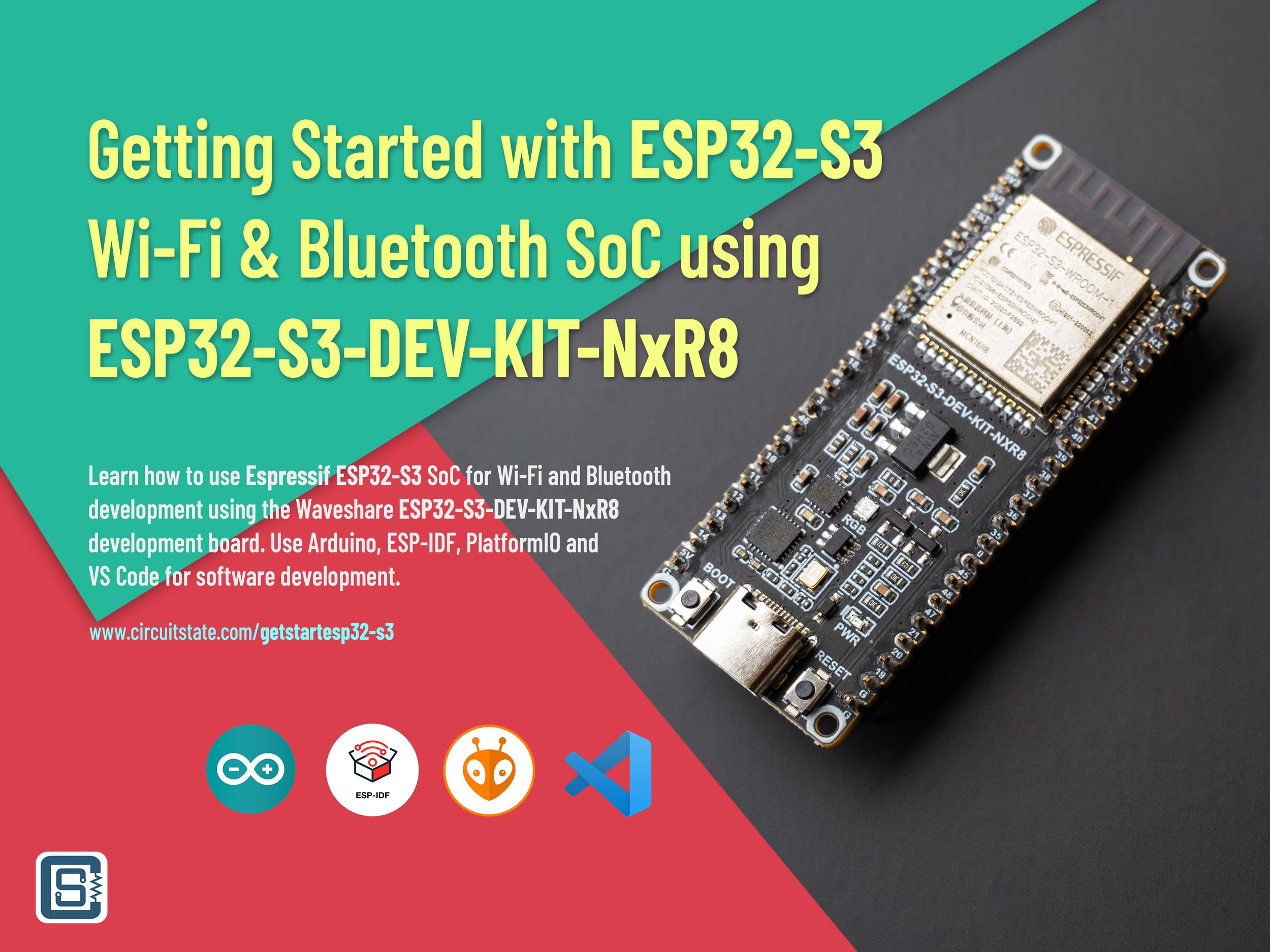
Getting Started with ESP32-S3 Wi-Fi & Bluetooth SoC using ESP32-S3-DEV-KIT-NxR8
Pinout Diagram
Filename: Waveshare-ESP32-S3-DEV-KIT-NXR8-Pinout-R0.1-CIRCUITSTATE-Electronics-1.pdf
Latest Revision: R0.1, 21-06-2025
Designed by: Vishnu Mohanan
License: CC-BY-SA 4.0
Pinouts are based on the latest documentation from Espressif. While we try our best to be accurate and up-to-date here, we can not guarantee correctness. Please also cross check the pin assignments with that from the official documentation. If you found any errors here, please let us know in the comments and will update our designs.
PNG
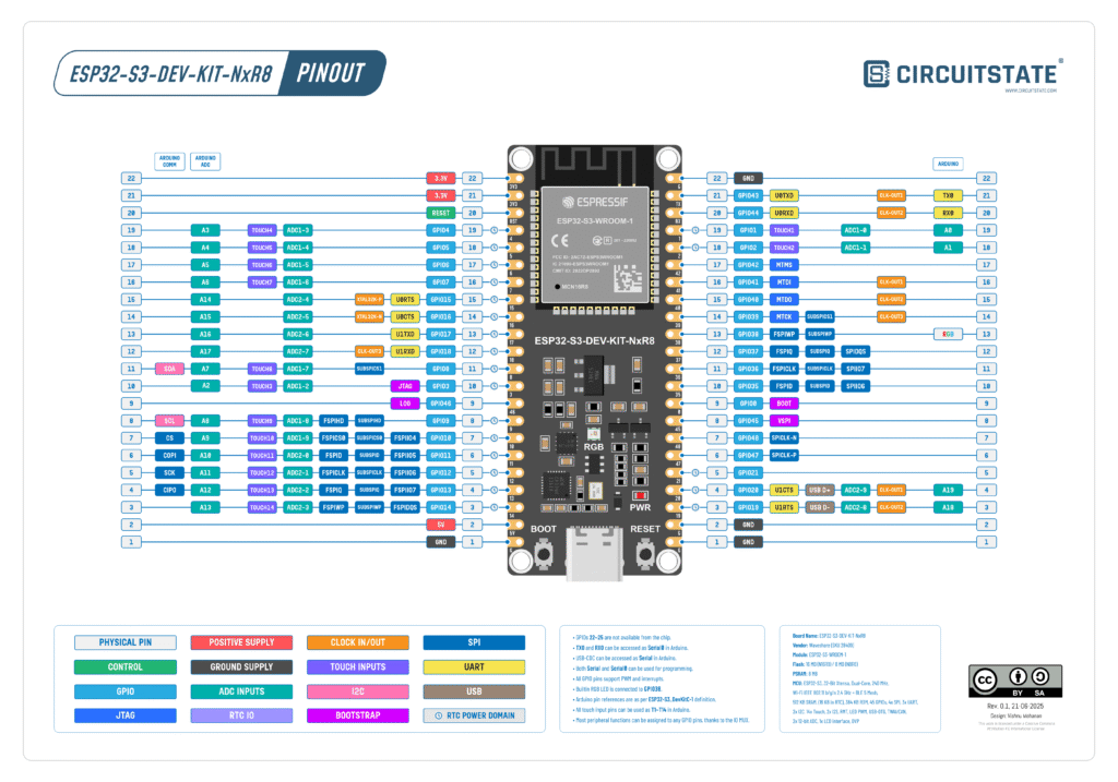
The ESP32-S3-DEV-KIT-NxR8 from Waveshare comes in two variants and 4 SKUs.
- ESP32-S3-DEV-KIT-N8R8 – Uses ESP32-S3-WROOM-1 module with 8 MB Flash memory and 8 MB PSRAM.
- ESP32-S3-DEV-KIT-N16R8 – Uses ESP32-S3-WROOM-1 module with 16 MB Flash memory and 8 MB PSRAM.
- Both of the above with and without soldered pin headers.
Our pinout is applicable for all of these. Since these boards did not come with an official pin numbering, there is no consensus over where to start counting from. So to make it easier for you to identify the pins by simply counting, we have numbered each row of pins on either side from 1 to 22. But you should not rely on the pin numbering alone to identify the pins. Always use the GPIO number to identify the pins and their functions.
Following are the notes added to the pinout diagram.
- GPIOs 22~25 are not available from the chip.
TX0andRX0can be accessed asSerial0in Arduino.- USB-CDC can be accessed as
Serialin Arduino. - Both
SerialandSerial0can be used for programming. - All GPIO pins support PWM and interrupts.
- Built-in RGB LED is connected to
GPIO38. - Arduino pin references are as per ESP32-S3_DevKitC-1 definition.
- All touch input pins can be used as T1~T14 in Arduino.
- Most peripheral functions can be assigned to any GPIO pins, thanks to the IO MUX.
PDF preview may not load on mobile devices. Click the link to open an interactive preview, or download it directly.
Pinout Reference
Power & Control
There are two positive power supply input pins and one control pin on the DOIT ESP32 DevKit V1.
| Pin Name | Function |
|---|---|
5V | The input of the 3.3V positive voltage regulator. Supply voltage in the range of 4 to 12V. |
3.3V | Output from the voltage regulator. You can also supply 3.3V to this pin if you have one. But do not supply both 5V and 3.3V together. |
GND | Ground (Negative) supply pins. |
RST | This is the reset pin. Connecting this pin to GND will reset the ESP32-S3. This pin is normally pulled-up. The RESET button on the board will pull it LOW when you press it. |
GPIO
There are 45 GPIO pins available on the ESP32-S3 chip. For comparison, the legacy ESP32 only had 34 GPIO pins. The GPIO pins are named from 0 to 48. But doesn’t that make the count 49? No, because GPIOs 22, 23, 24, and 25 are not accessible. So you will not find these pins in the table below. Also, not all of these pins are broken from the module or the board. But it is good to have a reference to know what is what. Below is the default ESP32-S3 GPIO function matrix taken from the official documentation. Note that many of the peripheral functions can be mapped to any of the GPIO pins using the GPIO Mux block of the ESP32.
| #Pin | GPIO Name | F0 | Type | F1 | Type | F2 | Type | F3 | Type | F4 | Type |
|---|---|---|---|---|---|---|---|---|---|---|---|
| 5 | GPIO0 | GPIO0 | I/O/T | GPIO0 | I/O/T | ||||||
| 6 | GPIO1 | GPIO1 | I/O/T | GPIO1 | I/O/T | ||||||
| 7 | GPIO2 | GPIO2 | I/O/T | GPIO2 | I/O/T | ||||||
| 8 | GPIO3 | GPIO3 | I/O/T | GPIO3 | I/O/T | ||||||
| 9 | GPIO4 | GPIO4 | I/O/T | GPIO4 | I/O/T | ||||||
| 10 | GPIO5 | GPIO5 | I/O/T | GPIO5 | I/O/T | ||||||
| 11 | GPIO6 | GPIO6 | I/O/T | GPI06 | I/O/T | ||||||
| 12 | GPIO7 | GPIO7 | I/O/T | GPIO7 | I/O/T | ||||||
| 13 | GPIO8 | GPIO8 | I/O/T | GPIO8 | I/O/T | SUBSPICS1 | O/T | ||||
| 14 | GPIO9 | GPIO9 | I/O/T | GPIO9 | I/O/T | SUBSPIHD | I1/O/T | FSPIHD | I1/O/T | ||
| 15 | GPIO10 | GPIO10 | I/O/T | GPIO10 | I/O/T | FSPIIO4 | I1/O/T | SUBSPICS0 | O/T | FSPICS0 | I1/O/T |
| 16 | GPIO11 | GPIO11 | I/O/T | GPIO11 | I/O/T | FSPIIO5 | I1/O/T | SUBSPID | I1/O/T | FSPID | I1/O/T |
| 17 | GPIO12 | GPIO12 | I/O/T | GPIO12 | I/O/T | FSPIIO6 | I1/O/T | SUBSPICLK | O/T | FSPICLK | I1/O/T |
| 18 | GPIO13 | GPIO13 | I/O/T | GPIO13 | I/O/T | FSPIIO7 | I1/O/T | SUBSPIQ | I1/O/T | FSPIQ | I1/O/T |
| 19 | GPIO14 | GPIO14 | I/O/T | GPIO14 | I/O/T | FSPIDQS | O/T | SUBSPIWP | I1/O/T | FSPIWP | I1/O/T |
| 21 | GPIO15 | GPIO15 | I/O/T | GPIO15 | I/O/T | U0RTS | O | ||||
| 22 | GPIO16 | GPIO16 | I/O/T | GPIO16 | I/O/T | U0CTS | I1 | ||||
| 23 | GPIO17 | GPIO17 | I/O/T | GPIO17 | I/O/T | U1TXD | O | ||||
| 24 | GPIO18 | GPIO18 | I/O/T | GPIO18 | I/O/T | U1RXD | I1 | CLK_OUT3 | O | ||
| 25 | GPIO19 | GPIO19 | I/O/T | GPIO19 | I/O/T | U1RTS | O | CLK_OUT2 | O | ||
| 26 | GPIO20 | GPIO20 | I/O/T | GPIO20 | I/O/T | U1CTS | I1 | CLK_OUT1 | O | ||
| 27 | GPIO21 | GPIO21 | I/O/T | GPIO21 | I/O/T | ||||||
| 28 | GPIO26 | SPICS1 | O/T | GPIO26 | I/O/T | ||||||
| 30 | GPIO27 | SPIHD | I1/O/T | GPIO27 | I/O/T | ||||||
| 31 | GPIO28 | SPIWP | I1/O/T | GPIO28 | I/O/T | ||||||
| 32 | GPIO29 | SPICS0 | O/T | GPIO29 | I/O/T | ||||||
| 33 | GPIO30 | SPICLK | O/T | GPIO30 | I/O/T | ||||||
| 34 | GPIO31 | SPIQ | I1/O/T | GPIO31 | I/O/T | ||||||
| 35 | GPIO32 | SPID | I1/O/T | GPIO32 | I/O/T | ||||||
| 38 | GPIO33 | GPIO33 | I/O/T | GPIO33 | I/O/T | FSPIHD | I1/O/T | SUBSPIHD | I1/O/T | SPIIO4 | I1/O/T |
| 39 | GPIO34 | GPIO34 | I/O/T | GPIO34 | I/O/T | FSPICS0 | I1/O/T | SUBSPICS0 | O/T | SPIIO5 | I1/O/T |
| 40 | GPIO35 | GPIO35 | I/O/T | GPIO35 | I/O/T | FSPID | I1/O/T | SUBSPID | I1/O/T | SPIIO6 | I1/O/T |
| 41 | GPIO36 | GPIO36 | I/O/T | GPIO36 | I/O/T | FSPICLK | I1/O/T | SUBSPICLK | O/T | SPIIO7 | I1/O/T |
| 42 | GPIO37 | GPIO37 | I/O/T | GPIO37 | I/O/T | FSPIQ | I1/O/T | SUBSPIQ | I1/O/T | SPIDQS | IO/O/T |
| 43 | GPIO38 | GPIO38 | I/O/T | GPIO38 | I/O/T | FSPIWP | I1/O/T | SUBSPIWP | I1/O/T | ||
| 44 | GPIO39 | MTCK | I1 | GPIO39 | I/O/T | CLK_OUT3 | O | SUBSPICS1 | O/T | ||
| 45 | GPIO40 | MTDO | O/T | GPIO40 | I/O/T | CLK_OUT2 | O | ||||
| 47 | GPIO41 | MTDI | I1 | GPIO41 | I/O/T | CLK_OUT1 | O | ||||
| 48 | GPIO42 | MTMS | I1 | GPIO42 | I/O/T | ||||||
| 49 | GPIO43 | U0TXD | O | GPIO43 | I/O/T | CLK_OUT1 | O | ||||
| 50 | GPIO44 | U0RXD | I1 | GPIO44 | I/O/T | CLK_OUT2 | O | ||||
| 51 | GPIO45 | GPIO45 | I/O/T | GPIO45 | I/O/T | ||||||
| 52 | GPIO46 | GPIO46 | I/O/T | GPIO46 | I/O/T | ||||||
| 37 | GPIO47 | SPI CLK_P_DIFF | O/T | GPIO47 | I/O/T | SUBSPI CLK_P_DIFF | O/T | ||||
| 36 | GPIO48 | SPI CLK_N_DIFF | O/T | GPIO48 | I/O/T | SUBSPI CLK_N_DIFF | O/T |
Each IO MUX function (Fn, n = 0 ~ 4) is associated with a type. The description of type is as follows:
- I – input. O – output. T – high impedance.
- I1 – input; if the pin is assigned a function other than Fn, the input signal of Fn is always
1. - I0 – input; if the pin is assigned a function other than Fn, the input signal of Fn is always
0.
Following is the consolidated pinout table of the ESP32-S3 taken from the official datasheet.
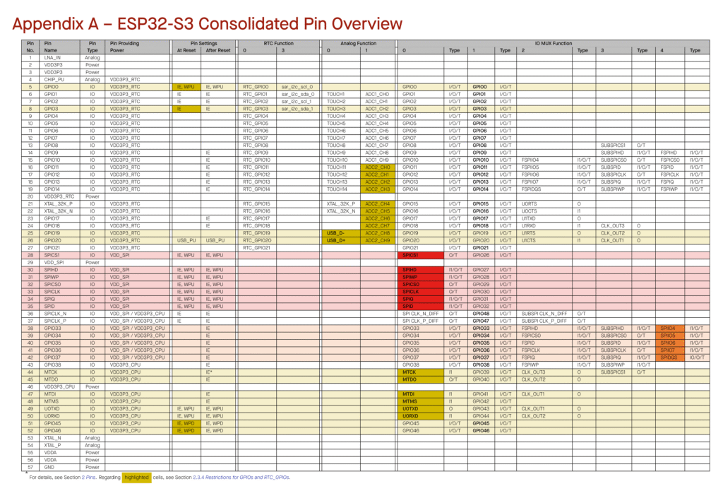
In the Arduino environment, you can invoke the GPIO pins just using their respective numbers from 0 to 48. Below is the list of pins you can use safely.
Strapping
Every ESP32-S3 chip has a bootloader inside the Read-Only-Memory (ROM) which is a program that monitors the state of the chip when you power it on. The bootloader can check for different inputs and put the chip into different operating modes. The pins monitored by the bootloader are called strapping pins. There are four strapping pins in the ESP32-S3. These strapping pins exhibit other behaviours during the booting process. So you should be careful not to interfere with the pins. Following is the list of strapping pins and their default states. It is recommended to not use these in normal situations.
| Strapping Pin | Default Configuration | Bit Value |
|---|---|---|
GPIO0 | Weak pull-up | 1 |
GPIO3 | Floating | – |
GPIO45 | Weak pull-down | 0 |
GPIO46 | Weak pull-down | 0 |
Chip Boot Mode Control
GPIO0 and GPIO46 together control the boot mode of the ESP32-S3. This tell the microcontroller where to load the firmware from.
| Boot Mode | GPIO0 | GPIO46 |
|---|---|---|
| SPI Boot | 1 | Any |
| Joint Download Boot | 0 | 0 |
SPI Boot is the default mode since GPIO0 pin is pulled-up by default. This means, the firmware will be loaded from the SPI Flash memory by default. Joint Download Boot mode supports the following download methods:
- USB Download Boot:
– USB-Serial-JTAG Download Boot
– USB-OTG Download Boot - UART Download Boot
VDD_SPI Voltage Control
The GPIO45 controls the VDD_SPI voltage for the SPI Flash interface. This allows you to use flash chips with different operating voltages. The state of EFUSE_VDD_SPI_FORCE and EFUSE_VDD_SPI_TIEH efuses also determines the voltage configuration. Please check the section 3.2 VDD_SPI Voltage Control in the ESP32-S3 datasheet for more information.
| VDD_SPI Power Source | Voltage | EFUSE_VDD_SPI_FORCE | GPI045 | EFUSE_VDD_SPI_TIEH |
|---|---|---|---|---|
| VDD3P3_RTC via RSPI | 3.3 V | 0 | 0 | Ignored |
| Flash Voltage Regulator | 1.8 V | 1 | ||
| Flash Voltage Regulator | 1.8 V | 1 | Ignored | 0 |
| VDD3P3_RTC via RSPI | 3.3 V | 1 |
ROM Messages Printing Control
During boot process the messages by the ROM code can be printed to:
- (Default)
UART0and USB Serial/JTAG controller - USB Serial/JTAG controller
UART0
The ROM messages printing to UART or USB Serial/JTAG controller can be respectively disabled by configuring
registers and eFuse. In the default configuration, GPIO46 is pulled-down and the boot messages are enabled. To disable the messages, simply pull the pin HIGH. For more information, please see the ESP32-S3 Technical Reference Manual > Chapter Chip Boot Control.
JTAG Signal Source Control
GPIO3 controls the source of JTAG signals during the early boot process. This GPIO is used together withEFUSE_DIS_PAD_JTAG, EFUSE_DIS_USB_JTAG, and EFUSE_STRAP_JTAG_SEL. Since the default state of the pin is floating, you can configure this manually to select the JTAG source. For more information, please see the ESP32-S3 Technical Reference Manual > Chapter Chip Boot Control.
| JTAG Signal Source | EFUSE_DIS_PAD_JTAG | EFUSE_DIS_USB_JTAG | EFUSE_STRAP_JTAG_SEL | GPI03 |
|---|---|---|---|---|
| USB Serial/ JTAG Controller | 0 | 0 | 0 | Ignored |
0 | 0 | 1 | 1 | |
1 | 0 | Ignored | Ignored | |
| JTAG Pins | 0 | 0 | 1 | 0 |
0 | 1 | Ignored | Ignored | |
| JTAG is disabled | 1 | 1 | Ignored | Ignored |
Pull-Up & Pull-Down
All GPIO pins support internal pull-up and pull-down configurations, as well as a high-impedance state. This makes the pin tristate compatible.
LED
The onboard WS2812B RGB LED is connected to GPIO38. Since this is serial RGB LED, you will need to use a compatible library to drive it. You can use the Adafruit Neopixel library for this.
USB
ESP32-S3 has a single USB transceiver that conforms to the USB 2.0 standard. It can support both Host and Device modes and therefore also supports USB-On-The-Go (USB-OTG). The maximum data rate is 12 Mbps. The USB pins of the ESP32-S3 are connected to the CH334F 4-port hub IC in the ESP32-S3-DEV-KIT-NxR8. When you connect the board to the computer, an interface with the name USB JTAG/serial debug unit will show up. This is the native USB interface.
| GPIO | USB |
|---|---|
GPIO20 | D+ |
GPIO19 | D- |
UART
ESP32-S3 has three UARTs inside (asynchronous only) with hardware and software flow control. The UARTs are named UART0, UART1, and UART2. In the ESP32-S3-DEV-KIT-NxR8, the UART0 is connected to the CH343P USB-UART chip, which in turn is connected to the CH334F 4-port USB hub IC. Therefore both the native USB interface as well as the UART0 port will be available through a single USB-C receptacle. Both the UART0 and the USB-CDC can be used for debugging and programming.
In the Arduino framework, you can access the UART0 as Serial0 and the native USB as Serial. Remapping of the UART pins can be done by passing the new pins to the begin() function. UART1 is mapped to Serial1 while UART2 to Serial2 but without any explicit pin assignments. All UART functions can be assigned to any GPIO pin. The default ones are listed below.
| Arduino Instance | UART | RX Pin | TX Pin | CTS | RTS |
|---|---|---|---|---|---|
Serial0 | UART0 | 44 (RX0) | 43 (TX0) | 16 | 15 |
Serial1 | UART1 | 18 (RX1) | 17 (TX1) | 20 | 19 |
Serial2 | UART2 | – | – | NA | NA |
SPI
There are four SPI peripheral blocks inside the ESP32-S3. SPI0 and SPI1 have special functions including communicating with the flash memory and therefore we don’t use them. SPI2 (GP-SPI2) and SPI3 (GP-SPI3) are general-purpose SPI interfaces called FSPI and HSPI respectively. Similar to the UART, SPI functions can be mapped to any GPIO pin. Below we have the default pins and their respective Arduino instances. Only one SPI is defined in the Arduino framework, but you can easily add the second one.
| Arduino Instance | SPI | COPI | CIPO | SCK | CS |
|---|---|---|---|---|---|
SPI2 | FSPI | – | – | – | – |
SPI3 | HSPI | 11 | 13 | 12 | 10 |
For some reason, the Arduino environment and the ESP32 HAL driver assign HSPI’s default pins to VSPI.
ADC
Analog to Digital Converters (ADC) are used to convert analog voltages to discrete digital values. There are two 12-bit SAR ADCs available in the ESP32-S3 with 20 input channels. Following is the list of ADC channels and their Arduino instances.
| Arduino Pin | ADC Channel | GPIO | Usable? |
|---|---|---|---|
A0 | ADC1_0 | 1 | YES |
A1 | ADC1_1 | 2 | YES |
A2 | ADC1_2 | 3 | YES |
A3 | ADC1_3 | 4 | YES |
A4 | ADC1_4 | 5 | YES |
A5 | ADC1_5 | 6 | YES |
A6 | ADC1_6 | 7 | YES |
A7 | ADC1_7 | 8 | YES |
A8 | ADC1_8 | 9 | YES |
A9 | ADC1_9 | 10 | YES |
A10 | ADC2_0 | 11 | YES |
A11 | ADC2_1 | 12 | YES |
A12 | ADC2_2 | 13 | YES |
A13 | ADC2_3 | 14 | YES |
A14 | ADC2_4 | 15 | YES |
A15 | ADC2_5 | 16 | YES |
A16 | ADC2_6 | 17 | YES |
A17 | ADC2_7 | 18 | YES |
A18 | ADC2_8 | 19 | NO (USB D-) |
A19 | ADC2_9 | 20 | NO (USB D+) |
Touch Sensor
There are 14 capacitive touch channels in the ESP3-S3.
| Arduino Pin | Touch Channel | GPIO | Usable? |
|---|---|---|---|
T1 | TOUCH1 | 1 | YES |
T2 | TOUCH2 | 2 | YES |
T3 | TOUCH3 | 3 | YES |
T4 | TOUCH4 | 4 | YES |
T5 | TOUCH5 | 5 | YES |
T6 | TOUCH6 | 6 | YES |
T7 | TOUCH7 | 7 | YES |
T8 | TOUCH8 | 8 | YES |
T9 | TOUCH9 | 9 | YES |
T10 | TOUCH10 | 10 | YES |
T11 | TOUCH11 | 11 | YES |
T12 | TOUCH12 | 12 | YES |
T13 | TOUCH13 | 13 | YES |
T14 | TOUCH14 | 14 | YES |
I2C
There are two I2C peripherals inside the ESP32-S3. I2C is also called as Two Wire Interface (TWI). Similar to UART and SPI, I2C pins can also be mapped to any GPIO pin. There are two I2C interfaces defined for Arduino; Wire (I2C0) and Wire1 (I2C1) but only Wire has the pins defined. You need to manually set the pins for Wire1.
| Arduino Instance | I2C | SDA | SCL |
|---|---|---|---|
Wire | I2C0 | 8 | 9 |
Wire1 | I2C1 | – | – |
PWM
ESP32-S3 supports up to 8 independent PWM (Pulse Width Modulation) channels with 14-bit precision. PWM outputs can be mapped to any GPIO pin that supports output mode.
I2S
Inter-Integrated Sound (I2S) is a digital audio interface supported by the ESP32-S3. I2S pin functions can also be mapped to any GPIO pins.
CAN/TWAI
Controller Area Network (CAN) or Two Wire Automotive Interface (TWAI) is a two-wire communication interface that mainly finds application in the automotive industry. CAN functions can be mapped to any GPIO pins. We have a complete tutorial for using CAN interface with ESP32.
What is CAN Bus & How to use CAN Interface with ESP32 and Arduino
JTAG
JTAG (Joint Test Action Group) is a standard interface used for programming and debugging microcontrollers. ESP32-S3 supports JTAG programming and debugging. JTAG has four main signals and an optional reset line. You can use supported debuggers like the ESP-Prog to debug your ESP chips.
| Pin Name | GPIO | Function |
|---|---|---|
MTDI | 41 | Test Data In |
MTCK | 39 | Test Clock |
MTMS | 42 | Test Mode Select |
MTDO | 40 | Test Data Out |
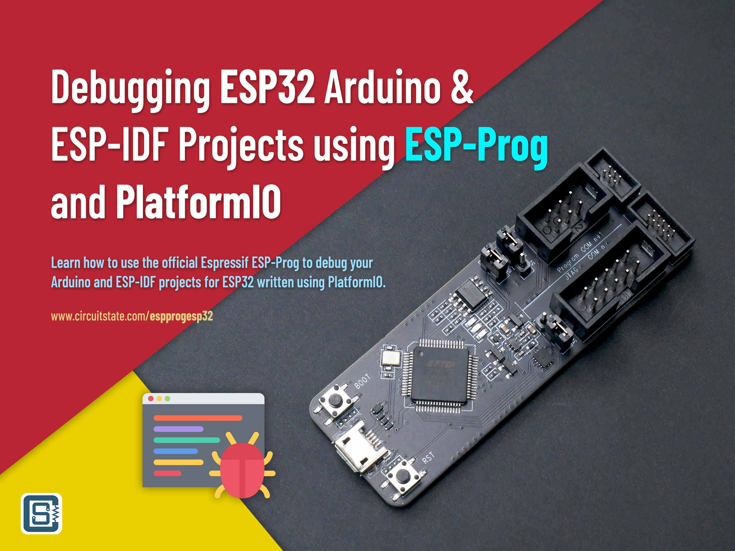
If you want to learn more about ESP32 debugging through the JTAG interface using the ESP-Prog, we have a complete tutorial for you.
Debugging ESP32 Arduino & ESP-IDF Projects using ESP-Prog and PlatformIO
External Interrupts
ESP32-S3 supports external interrupts on all GPIO pins. The interrupt types can be level-triggered, edge-triggered, or state change.
Links
- ESP32-S3 – Product Page
- ESP32-S3 Technical Reference Manual [PDF]
- ESP32-S3 Datasheet [PDF]
- ESP32-S3 – ESP-IDF Programming Guide
- ESP32-S3 Bootloader and Strapping Pins
- Introduction to the ESP-Prog Board
- Waveshare ESP32-S3-DEV-KIT-N8R8 – Wiki
- Waveshare ESP32-S3-DEV-KIT-N8R8 – Product Page
Short Link
- Short URL to this page – https://circuitstate.com/wsesp32s3dkpinref
