Raspberry Pi Pico RP2040 Microcontroller Board – Pinout Diagram & Arduino Pin Reference
Beautiful pinout diagram for the Raspberry Pico RP2040 microcontroller boards, in both PNG and PDF formats, and Arduino pin reference.
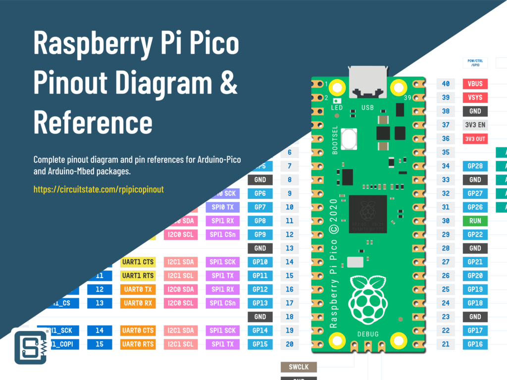
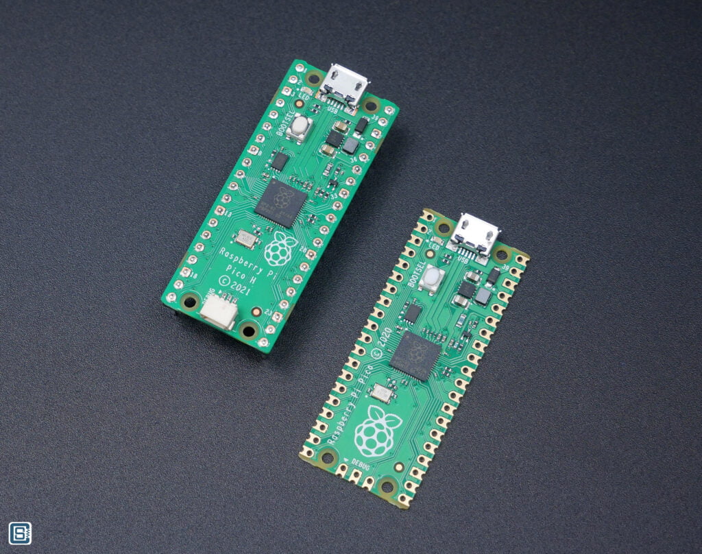
The Raspberry Pi Pico is a small form-factor development board and PCB module based on the RP2040 dual-core microcontroller from the Raspberry Pi Foundation, UK. Based on the form-factor of a 40-pin DIP IC package, the board can be plugged onto a breadboard or soldered on a PCB using the castellated holes. On this page, you will find the pinout diagrams and references for the Raspberry Pi Pico board designed by CIRCUITSTATE. If you want to learn more about the RP2040 microcontroller, we have a getting started tutorial below.
Getting Started with Raspberry Pi Pico : RP2040 Microcontroller Board – Pinout, Schematic and Programming Tutorial
We can develop embedded firmware for you
CIRCUITSTATE can develop embedded firmware for any microcontroller/microprocessor including 8051, PIC, AVR, ARM, STM32, ESP32, and RISC-V using industry-leading SDKs, frameworks, and tools. Contact us today to share your requirements.

Pinout Diagram
The Raspberry Pi Pico has an official pinout diagram here. But we thought we could a better job at designing one ourselves that also includes the Arduino pin names. You are free to download, modify and redistribute the design under Creative Commons Attribution 4.0 International License. This pinout is also applicable for other board variants such as Raspberry Pi Pico H, W, and the WIZnet WizFi360 Pico.
Latest Revision: R0.3, 06-12-2022
Designed by: Vishnu Mohanan
License: CC-BY-SA 4.0
Pinouts are based on the latest documentation from Raspberry Pi. While we try our best to be accurate and up-to-date here, we can not guarantee correctness. Please also cross-check the pin assignments with that from the official documentation. If you found any errors here, please let us know in the comments and we will update our designs.
PNG
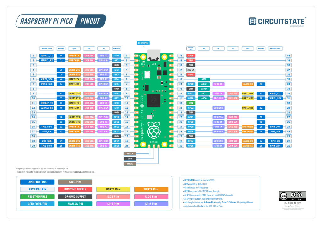
License: CC-BY-SA by CIRCUITSTATE Electronics.
PDF preview may not load on mobile devices. Click the link to open an interactive preview, or download it directly.
Old Versions
- Revision 0.1 – Raspberry-Pi-Pico-Pinout-R0.1-CIRCUITSTATE-Electronics.pdf
- Revision 0.2 – Raspberry-Pi-Pico-Pinout-R0.2-CIRCUITSTATE-Electronics.pdf
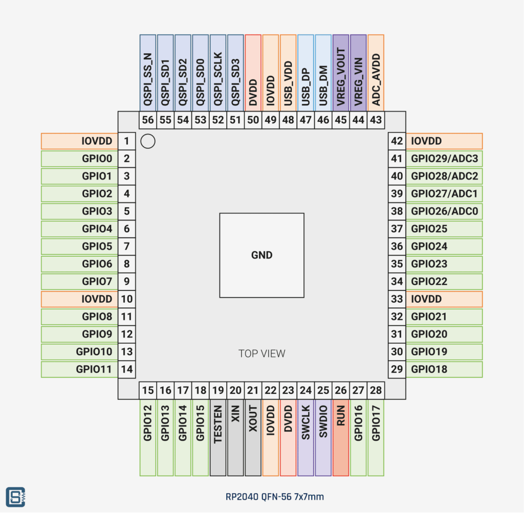
RP2040 Pinout
Pinout Reference
Power & Control
Here is a list of pins used to supply power, clock, and other control signals. Pins with similar names are internally connected together and it is also recommended to connect them externally when designing a PCB.
| Name | Pins | Description |
|---|---|---|
IOVDD | 1, 10, 22, 33, 42, 49 | Power supply for digital GPIOs, nominal voltage 1.8V to 3.3V |
DVDD | 23, 50 | Digital core power supply, nominal voltage 1.1V. Can be connected to VREG_VOUT, or to some other board-level power supply. |
ADC_AVDD | 43 | Power supply for analogue-to-digital converter, nominal voltage 3.3V |
USB_VDD | 48 | Power supply for internal USB Full Speed PHY, nominal voltage 3.3V |
VREG_VIN | 44 | Power input for the internal core voltage regulator, nominal voltage 1.8V to 3.3V |
VREG_VOUT | 45 | Power output for the internal core voltage regulator, nominal voltage 1.1V, 100mA max current |
GND | Exposed Pad (EP) | Single external ground connection, bonded to a number of internal ground pads on the RP2040 die. |
RUN | 26 | Global asynchronous reset pin. Reset when driven low, run when driven high. If no external reset is required, this pin can be tied directly to IOVDD. |
TESTEN | 19 | Factory test mode pin. Tie to GND. |
XIN and XOUT | 20, 21 | Connect a crystal to RP2040’s crystal oscillator. XIN can also be used as a single-ended CMOS clock input, with XOUT disconnected. The USB bootloader requires a 12MHz crystal or 12MHz clock input. |
Memory
These pins are used to interface an external flash memory since RP2040 does not have an internal flash capacity. A Quad SPI (SPI with four data lines) interface is used for the flash interface. The QSPI pins can also be used as GPIOs if not being used to interface the flash.
| Name | Pins | Description |
|---|---|---|
QSPI_SD3 | 51 | Serial Data 3 |
QSPI_SCLK | 52 | Serial Clock |
QSPI_SD0 | 53 | Serial Data 0 |
QSPI_SD2 | 54 | Serial Data 2 |
QSPI_SD1 | 55 | Serial Data 1 |
QSPI_SS_N | 56 | SPI Chip Select |
SWD
Serial Wire Debug (SWD) is the interface used to program and debug the RP2040 microcontroller. Only three pins (including GND) are required for this interface and they can not be used for anything else.
| Name | Pins | Description |
|---|---|---|
| SWCLK | 24 | SWD Clock |
| SWDIO | 25 | SWD Data In and Out |
USB
RP2040 contains a single USB 2.0 controller that can act as both host and peripheral. But the speeds are limited to Low-Speed (1.5 Mbps) and Full-Speed (12 Mbps) due to the usage of a USB 1.1 PHY (Physical Layer). When wiring up a USB connector, you need at least four lines; DP, DM, VBUS, and GND. VBUS is a +5V supply sourced by an external host when RP2040 is in peripheral mode. You can use it to power the microcontroller. In USB host mode, you must use the VBUS to supply +5V to the connected device.
The USB data lines can not be used for anything else and should be left floating if not used.
| Name | Pins | Description |
|---|---|---|
| USB_DP | 47 | USB Data Positive (D+) |
| USB_DM | 46 | USB Data Negative (D-) |
GPIO Function Matrix
The RP2040 has 30 General Purpose Input/Output (GPIO) pins; an odd number indeed. This set of pins is referred to as Bank 0 in the datasheet. Maybe we will get an additional Bank 1 with a newer version of RP2040. GPIO pins also have special functions other than the digital input and output which are listed below.
| GPIO | F1 | F2 | F3 | F4 | F5 | F6 | F7 | F8 | F9 |
|---|---|---|---|---|---|---|---|---|---|
| 0 | SPI0 RX | UART0 TX | I2C0 SDA | PWM0 A | SIO | PIO0 | PIO1 | USB OVCUR DET | |
| 1 | SPI0 CSn | UART0 RX | I2C0 SCL | PWM0 B | SIO | PIO0 | PIO1 | USB VBUS DET | |
| 2 | SPI0 SCK | UART0 CTS | I2C1 SDA | PWM1 A | SIO | PIO0 | PIO1 | USB VBUS EN | |
| 3 | SPI0 TX | UART0 RTS | I2C1 SCL | PWM1 B | SIO | PIO0 | PIO1 | USB OVCUR DET | |
| 4 | SPI0 RX | UART1 TX | I2C0 SDA | PWM2 A | SIO | PIO0 | PIO1 | USB VBUS DET | |
| 5 | SPI0 CSn | UART1 RX | I2C0 SCL | PWM2 B | SIO | PIO0 | PIO1 | USB VBUS EN | |
| 6 | SPI0 SCK | UART1 CTS | I2C1 SDA | PWM3 A | SIO | PIO0 | PIO1 | USB OVCUR DET | |
| 7 | SPI0 TX | UART1 RTS | I2C1 SCL | PWM3 B | SIO | PIO0 | PIO1 | USB VBUS DET | |
| 8 | SPI1 RX | UART1 TX | I2C0 SDA | PWM4 A | SIO | PIO0 | PIO1 | USB VBUS EN | |
| 9 | SPI1 CSn | UART1 RX | I2C0 SCL | PWM4 B | SIO | PIO0 | PIO1 | USB OVCUR DET | |
| 10 | SPI1 SCK | UART1 CTS | I2C1 SDA | PWM5 A | SIO | PIO0 | PIO1 | USB VBUS DET | |
| 11 | SPI1 TX | UART1 RTS | I2C1 SCL | PWM5 B | SIO | PIO0 | PIO1 | USB VBUS EN | |
| 12 | SPI1 RX | UART0 TX | I2C0 SDA | PWM6 A | SIO | PIO0 | PIO1 | USB OVCUR DET | |
| 13 | SPI1 CSn | UART0 RX | I2C0 SCL | PWM6 B | SIO | PIO0 | PIO1 | USB VBUS DET | |
| 14 | SPI1 SCK | UART0 CTS | I2C1 SDA | PWM7 A | SIO | PIO0 | PIO1 | USB VBUS EN | |
| 15 | SPI1 TX | UART0 RTS | I2C1 SCL | PWM7 B | SIO | PIO0 | PIO1 | USB OVCUR DET | |
| 16 | SPI0 RX | UART0 TX | I2C0 SDA | PWM0 A | SIO | PIO0 | PIO1 | USB VBUS DET | |
| 17 | SPI0 CSn | UART0 RX | I2C0 SCL | PWM0 B | SIO | PIO0 | PIO1 | USB VBUS EN | |
| 18 | SPI0 SCK | UART0 CTS | I2C1 SDA | PWM1 A | SIO | PIO0 | PIO1 | USB OVCUR DET | |
| 19 | SPI0 TX | UART0 RTS | I2C1 SCL | PWM1 B | SIO | PIO0 | PIO1 | USB VBUS DET | |
| 20 | SPI0 RX | UART1 TX | I2C0 SDA | PWM2 A | SIO | PIO0 | PIO1 | CLOCK GPIN0 | USB VBUS EN |
| 21 | SPI0 CSn | UART1 RX | I2C0 SCL | PWM2 B | SIO | PIO0 | PIO1 | CLOCK GPOUT0 | USB OVCUR DET |
| 22 | SPI0 SCK | UART1 CTS | I2C1 SDA | PWM3 A | SIO | PIO0 | PIO1 | CLOCK GPIN1 | USB VBUS DET |
| 23 | SPI0 TX | UART1 RTS | I2C1 SCL | PWM3 B | SIO | PIO0 | PIO1 | CLOCK GPOUT1 | USB VBUS EN |
| 24 | SPI1 RX | UART1 TX | 12C0 SDA | PWM4 A | SIO | PIO0 | PIO1 | CLOCK GPOUT2 | USB OVCUR DET |
| 25 | SPI1 CSn | UART1 RX | I2C0 SCL | PWM4 B | SIO | PIO0 | PIO1 | CLOCK GPOUT3 | USB VBUS DET |
| 26 | SPI1 SCK | UART1 CTS | I2C1 SDA | PWM5 A | SIO | PIO0 | PIO1 | USB VBUS EN | |
| 27 | SPI1 TX | UART1 RTS | I2C1 SCL | PWM5 B | SIO | PIO0 | PIO1 | USB OVCUR DET | |
| 28 | SPI1 RX | UART0 TX | I2C0 SDA | PWM6 A | SIO | PIO0 | PIO1 | USB VBUS DET | |
| 29 | SPI1 CSn | UART0 RX | I2C0 SCL | PWM6 B | SIO | PIOO | PIO1 | USB VBUS EN |
| Function Name | Description |
|---|---|
| SPIx | Connect one of the internal PL022 SPI peripherals to GPIO |
| UARTx | Connect one of the internal PL011 UART peripherals to GPIO |
| I2Cx | Connect one of the internal DW I2C peripherals to GPIO |
| PWMx A/B | Connect a PWM slice to GPIO. There are eight PWM slices, each with two output channels (A/B). The B pin can also be used as an input, for frequency and duty cycle measurement. |
| SIO | Software control of GPIO, from the single-cycle IO (SIO) block. The SIO function (F5) must be selected for the processors to drive a GPIO, but the input is always connected, so software can check the state of GPIOs at any time. |
| PIOx | Connect one of the programmable IO blocks (PIO) to GPIO. PIO can implement a wide variety of interfaces, and has its own internal pin mapping hardware, allowing flexible placement of digital interfaces on bank 0 GPIOs. The PIO function (F6, F7) must be selected for PIO to drive a GPIO, but the input is always connected, so the PIOs can always see the state of all pins. |
| CLOCK GPINx | General purpose clock inputs. Can be routed to a number of internal clock domains on RP2040, e.g. to provide a 1Hz clock for the RTC, or can be connected to an internal frequency counter. |
| CLOCK GPOUTx | General purpose clock outputs. Can drive a number of internal clocks (including PLL outputs) onto GPIOs, with optional integer divide. |
| USB OVCUR DET, VBUS DET, VBUS EN | USB power control signals to/from the internal USB controller |
Arduino-Pico
Here we have a list of pins that you can use in your Arduino sketches if you are using the Arduino-Pico core from Earle F. Philhower, III (@earlephilhower). These references are taken from the pins_arduino.h file.
GPIO
The 30 GPIO pins can be referenced from 0 to 29 in your Arduino sketch. But among the 30 pins, only 26 are broken out on the official Pico boards. A few of the pins are used for different control and measurement tasks. You can also reference the GPIO pins with the D prefix, eg. D21. All GPIO pins have pull-up and pull-down resistors associated with them which you can enable from the software.
- GP29/ADC3 is used to measure VSYS.
- GP25 is used by the debug LED.
- GP24 is used for VBUS sense.
- GP23 is connected to the SMPS Power Save pin.
LED
The onboard LED is connected to GPIO25.
UART
RP2040 has two dedicated UART ports (UART0 and UART1) with flow control pins. Functions of both UART instances can be assigned to multiple pins which are listed below. Additionally, the USB port can be enumerated as USB-CDC serial port which is the default Serial of Raspberry Pi Pico boards. The hardware UARTs can be invoked as Serial1 (UART0) and Serial2 (UART1). There are default pins assignments for both UARTs. But these pin assignments can be changed to other valid pins using setRX() and setTX() functions as described here. The alternative pins are given inside the brackets.
Additionally, you can use the PIO blocks to implement additional UARTs if needed.
| Arduino Instance | RX | TX | RTS | CTS |
|---|---|---|---|---|
Serial1 (UART0) | 1 (13, 17, 29) | 0 (12, 16, 28) | 3, 15, 19 | 2, 14, 18 |
Serial2 (UART1) | 9 (5, 21, 25) | 8 (4, 20, 24) | 7, 11, 23, 27 | 6, 10, 22, 26 |
SPI
There are two hardware SPI peripherals inside the RP2040. Similar to the UARTs, we can assign SPI functions to multiple sets of pins. Below is a list of default pins and alternative pins you can use in your Arduino sketches. You can change the pins using setRX(), setTX(), setCTS() and setSCK() functions as described here.
Additionally, you can use the PIO blocks to implement extra SPI interfaces if needed.
| Arduino Instance | SCK | COPI | CIPO | CS |
|---|---|---|---|---|
SPI (SPI0) | 18 (2, 6, 22) | 19 (3, 7, 23) | 16 (0, 4, 20) | 17 (1, 5, 21) |
SPI1 (SPI1) | 14 (10, 26) | 15 (11, 27) | 12 (8, 24, 28) | 13 (9, 25, 29) |
I2C
RP2040 has two I2C (Two Wire Interface) peripherals inside. These interfaces are referenced as Wire (I2C0) and Wire1 (I2C1) in the Arduino sketches. There are default pin assignments as well as alternative pins you can assign with functions setSCL() and setSDA() as explained here.
| Arduino Instance | SDA | SCL |
|---|---|---|
Wire (I2C0) | 4 (0, 8, 12, 16, 20, 24, 28) | 5 (1, 9, 13, 17, 21, 25, 29) |
Wire1 (I2C1) | 26 (2, 6, 10, 14, 18, 22) | 27 (3, 7, 11, 15, 19, 23, 27) |
PWM
RP2040’s PWM block has 8 slices. Each slice can drive up to 2 pins. That gives you 16 individually controlled PWM pins with 16-bit precision. All GPIO pins can be used for PWM output.
ADC
RP2040 has a single SAR ADC block inside with a maximum sampling rate of 500 ksps and a 12-bit precision. GPIO pins 26 to 29 can act as ADC inputs. In the Arduino framework, these pins have references as shown below.
| Arduino Pin | GPIO |
|---|---|
| A0 | 26 |
| A1 | 27 |
| A2 | 28 |
| A3 | 29 |
External Interrupts
RP2040 supports level (HIGH and LOW) and edge (rising and falling) triggered interrupts on all GPIO pins.
PIO
There are two identical Programmable IO (PIO) blocks inside the RP2040, each block with four state machines. The PIO block can be configured as a variety of hardware peripherals such as SPI, UART, SDIO, I2C, etc. All 30 GPIOs of the RP2040 can be used for PIO functions.
Arduino Mbed
There are two framework implementations for working with RP2040 in an Arduino environment. The Arduino-Pico core is maintained by Earle F. Philhower, III (@earlephilhower) and is based on the official RP2040 C/C++ SDK. Another one is the Arduino-Mbed package based on the open-source Mbed OS for microcontrollers. RP2040 pin assignments are different for both packages. Here we have the RP2040 pin assignments for the Arduino-Mbed.
GPIO
The GPIO pins can be referenced in the same way we did before, starting from 0 to 29.
UART
Only one UART is available in the Arduino-Mbed package for Raspberry Pi Pico, Serial1. The default Serial is the USB-CDC port.
| Arduino Instance | RX | TX |
|---|---|---|
Serial1 | 1 | 0 |
SPI
Only one SPI instance is available in the Arduino-Mbed package; SPI.
| Arduino Instance | SCK | COPI | CIPO | CS |
|---|---|---|---|---|
SPI | 18 | 19 | 16 | 17 |
I2C
Only one I2C instance is available.
| Arduino Instance | SDA | SCL |
|---|---|---|
Wire | 4 | 5 |
ADC
ADC pin assignments are the same for Arduino-Pico and Arduino-Mbed packages for Raspberry Pi Pico.
| Arduino Pin | GPIO |
|---|---|
| A0 | 26 |
| A1 | 27 |
| A2 | 28 |
| A3 | 29 |
Links
- Raspberry Pi Pico Datasheet
- RP2040 Datasheet
- Getting Started with Raspberry Pi Pico : RP2040 Microcontroller Board – Pinout, Schematic and Programming Tutorial
Short Link
- Short URL to this page: https://circuitstate.com/rpipicopinout



Great RP2040 summary!
You wrote:
“RP2040 contains a single USB 2.0 controller”
It’s wrong! it only have a USB 1.1 full-speed (12 Mbit/s).
We all wish it have a USB2.0 high-speed (480 Mbit/s)..
Also on the “GPIO Function Matrix” table, on column “F3”
you wrote “12C” instead of “I2C”.
Hope you can fix it and make another page for the new RP2350 family!
Thanks,
Arad 🙂
Thanks for your feedback and observations 🫡
As per the RP2040 datasheet, Chapter 4.1, the RP2040 contains a USB 2.0 compliant controller. But the interface is limited to Low-Speed (1.5 Mbps) and Full-Speed (12 Mbps) due to the use of a USB 1.1 PHY. So the speed limitation comes from the USB-PHY being used and not the controller. Since USB 2.0 is backward compatible with USB 1.0 and 1.1, the USB 2.0 controller on the RP2040 can take advantage of the new controller features, but at a lower maximum data rate. We have added note on the speed limitation to avoid the confusion.
We have changed the “12C” to “I2C”. This happens when we convert tables in the form of images to HTML tables.
We are already working on the RP2350 pinouts.